Unlock instant, AI-driven research and patent intelligence for your innovation.

Pixel structure, driving method thereof, display panel and display device

A technology of pixel structure and pixel circuit, applied in static indicators, instruments, etc., can solve problems such as difficult battery charging

Active Publication Date: 2018-09-28
BOE TECH GRP CO LTD
View PDF10 Cites 4 Cited by
  • Summary
  • Abstract
  • Description
  • Claims
  • Application Information

AI Technical Summary

Problems solved by technology

However, the photovoltaic voltage of the organic heterojunction in the existing pixel circuit is between 0.5 and 1.2V, which is difficult to charge the battery

Method used


Image

  • Pixel structure, driving method thereof, display panel and display device
  • Pixel structure, driving method thereof, display panel and display device
  • Pixel structure, driving method thereof, display panel and display device

Examples


Embodiment Construction

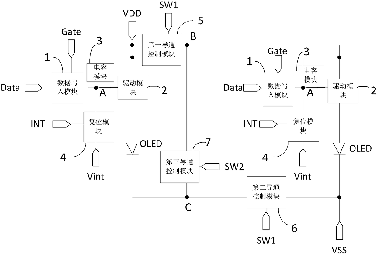
[0042] The specific implementations of the pixel structure and its driving method, the display panel and the display device provided by the embodiments of the present invention will be described in detail below with reference to the accompanying drawings.

[0043] A pixel structure provided by an embodiment of the present invention, such as figure 1As shown, it includes at least two identical pixel circuits: a first pixel circuit and a second pixel circuit, and also includes a first conduction control module 5 and a second conduction control module for connecting the first pixel circuit and the second pixel circuit. Module 6 and the third conduction control module 7;

[0044] Both the first pixel circuit and the second pixel circuit include: a data writing module 1, a driving module 2, a capacitor module 3, a reset module 4 and a light emitting device OLED;

[0045] The data module is used to provide the signal of the data signal terminal Data to the first node A under the co...


PUM


Abstract

The invention discloses a pixel structure, a driving method thereof, a display panel and a display device. The pixel structure comprises at least two identical pixel circuits including a first pixel circuit and a second pixel circuit, and the pixel structure further comprises a first conduction control module, a second conduction control module and a third conduction control module which are usedfor connecting the first pixel circuit and the second pixel circuit. When the pixel structure is used for display, the first conduction control module and the second conduction control module are under control of a first control end, the first pixel circuit and the second pixel circuit are connected in parallel, and light emission between the pixel circuits is not affected. When the pixel structure is used for photoelectric conversion to form a solar cell, the third conduction control module is under control of a second control end, the pixel circuits are connected in series, correspondingly photovoltaic voltage of light emitting devices is superimposed to achieve voltage for charging a battery, and therefore the pixel structure can achieve composite functions of pixel display and photoelectric conversion to form the solar cell.

Description

technical field [0001] The present invention relates to the technical field of electroluminescence, in particular to a pixel structure and a driving method thereof, a display panel and a display device. Background technique [0002] Organic Light Emitting Diode (OLED) is one of the hot spots in the field of flat panel display research today. Compared with liquid crystal displays, OLED has the advantages of low energy consumption, low production cost, self-illumination, wide viewing angle and fast response speed. , OLEDs have begun to replace traditional Liquid Crystal Displays (LCDs) in the field of flat panel displays such as mobile phones, PDAs, and digital cameras. Among them, pixel circuit design is the core technical content of OLED display, which has important research significance. [0003] Moreover, OLED is based on the structure of organic semiconductor heterojunction. This structure exhibits luminescence characteristics at positive bias voltage and photoelectric c...

Claims


Application Information

Patent Timeline
IPC IPC(8): G09G3/3208
CPCG09G3/3208G09G2330/00G09G3/3233G09G2300/0842G09G2300/0819G09G2310/0251G09G2300/0814G09G2330/023G09G2300/0804G09G3/3258G09G2300/0439G09G2310/061
Inventor 陈亮王磊肖丽刘冬妮玄明花陈小川杨盛际赵德涛
Owner BOE TECH GRP CO LTD