

Array substrate and manufacturing method thereof
A technology of an array substrate and a manufacturing method, which is applied in the field of flat panel displays, can solve problems such as abnormal display images and signal delays of display panels, and achieves the effect of solving signal delays and ensuring normal display.
- Summary
- Abstract
- Description
- Claims
- Application Information
AI Technical Summary
Problems solved by technology
Method used
Image

Examples
Embodiment Construction
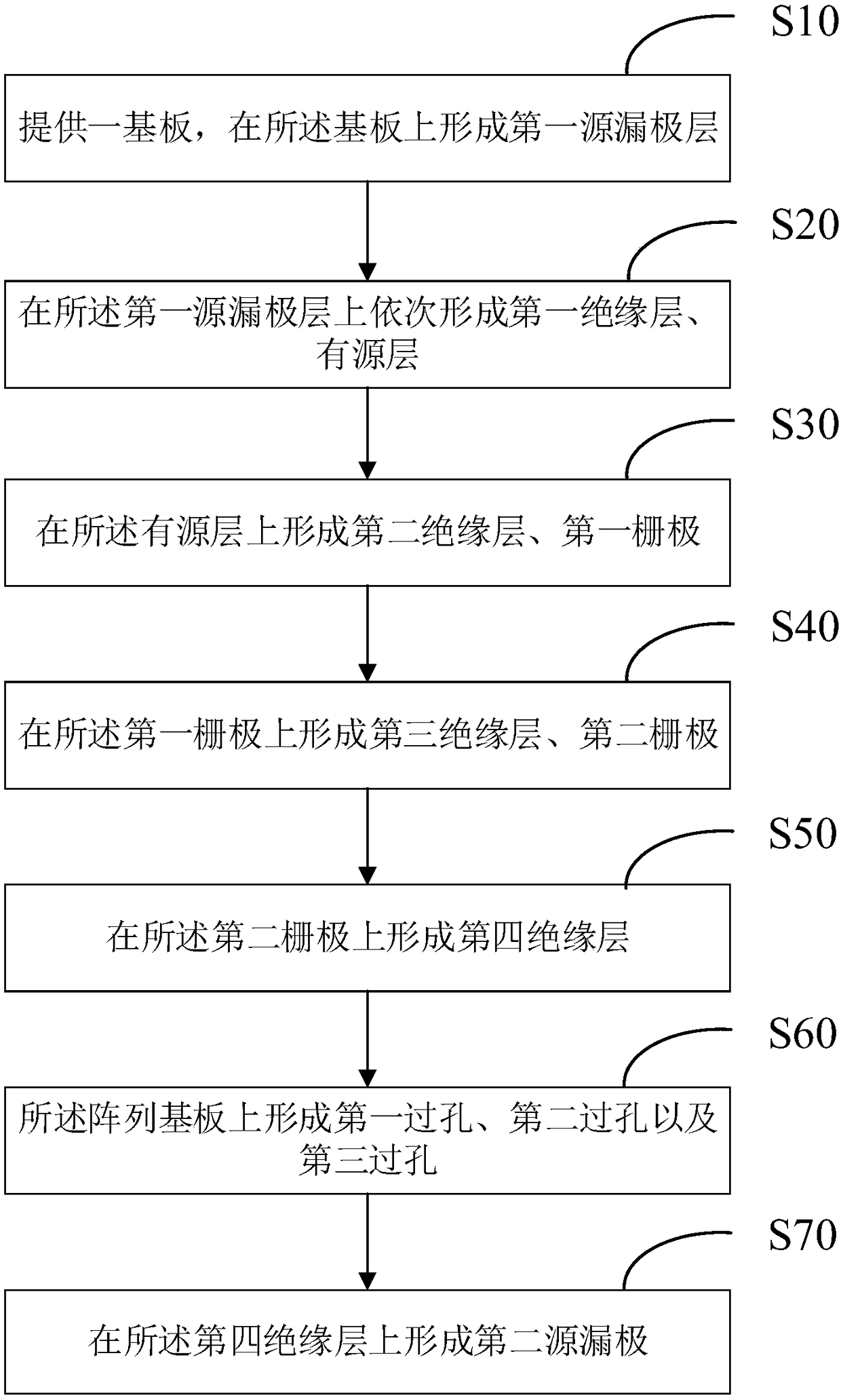
[0047] The following descriptions of the various embodiments refer to the accompanying drawings to illustrate specific embodiments in which the invention may be practiced. The directional terms mentioned in the present invention, such as [top], [bottom], [front], [back], [left], [right], [inside], [outside], [side], etc., are only for reference The orientation of the attached schema. Therefore, the directional terms used are used to illustrate and understand the present invention, but not to limit the present invention. In the figures, structurally similar elements are denoted by the same reference numerals.
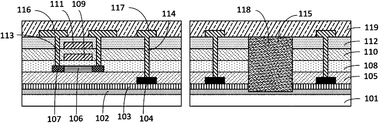
[0048] figure 1 Shown is an array substrate according to a preferred embodiment of the present invention, wherein the array substrate includes:
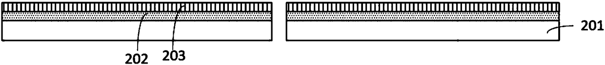
[0049] The substrate 101, the raw material of the substrate 101 may be one of a glass substrate, a quartz substrate, a resin substrate, and the like.
[0050] Flexible substrate film layer 102, the flexible substrate film l...
PUM
 Abstract
Description
Claims
Application Information