Thin film transistor, array substrate and display apparatus

A technology of thin film transistors and transparent substrates, applied in transistors, electric solid state devices, semiconductor devices, etc., can solve the problems of lowering the display quality of display devices, flickering of display images, afterimages and grayscale confusion, etc., so as to improve display quality and reduce feedback. The effect of the voltage

Inactive Publication Date: 2018-09-28
KUSN INFOVISION OPTOELECTRONICS
View PDF3 Cites 4 Cited by
  • Summary
  • Abstract
  • Description
  • Claims
  • Application Information

AI Technical Summary

Problems solved by technology

[0006] Feed-through voltage will cause problems such as flickering, afterimages, and grayscal

Method used


Image

  • Thin film transistor, array substrate and display apparatus
  • Thin film transistor, array substrate and display apparatus
  • Thin film transistor, array substrate and display apparatus

Examples


no. 1 example

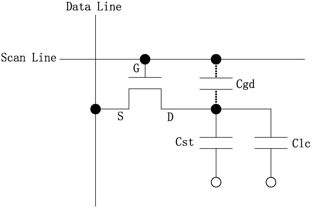
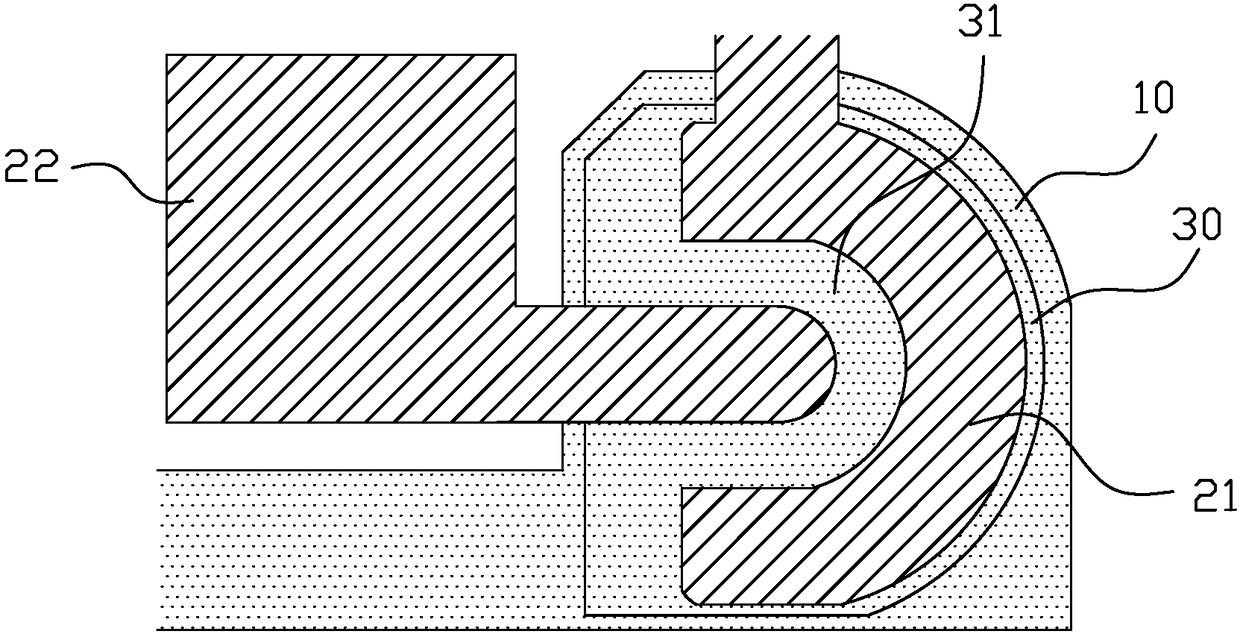
[0035] Please refer to Figure 3 to Figure 6 The thin film transistor provided by the first embodiment of the present invention includes a gate 110 , a source-drain metal layer 120 and a semiconductor layer 300 disposed on a transparent substrate 100 . Wherein, the gate 110 is arranged on the transparent substrate 100; the gate insulating layer 101 is also provided on the transparent substrate 100 to cover the gate 110; the semiconductor layer 300 is arranged on the gate insulating layer 101 and is located above the gate 110; The drain metal layer 120 is disposed on the semiconductor layer 300, including a source electrode 121 and a drain electrode 122. The source electrode 121 and the drain electrode 122 are separated from each other and are in contact with the semiconductor layer 300. The semiconductor layer 300 is provided with a channel 301, and the channel 301 is provided with between the source 121 and the drain 122 .

[0036]The source 121 is a "U"-shaped or "C"-shaped...

no. 2 example

[0047] Please refer to Figure 7 to Figure 10 , The thin film transistor provided by the second embodiment of the present invention includes a gate 110 , a source-drain metal layer 120 and a semiconductor layer 300 disposed on a transparent substrate 100 . Wherein, the gate 110 is arranged on the transparent substrate 100; the gate insulating layer 101 is also provided on the transparent substrate 100 to cover the gate 110; the semiconductor layer 300 is arranged on the gate insulating layer 101 and is located above the gate 110; The drain metal layer 120 is disposed on the semiconductor layer 300, including a source electrode 121 and a drain electrode 122. The source electrode 121 and the drain electrode 122 are separated from each other and are in contact with the semiconductor layer 300. The semiconductor layer 300 is provided with a channel 301, and the channel 301 is provided with between the source 121 and the drain 122 .

[0048] The source 121 is a "U"-shaped or "C"-s...

no. 3 example

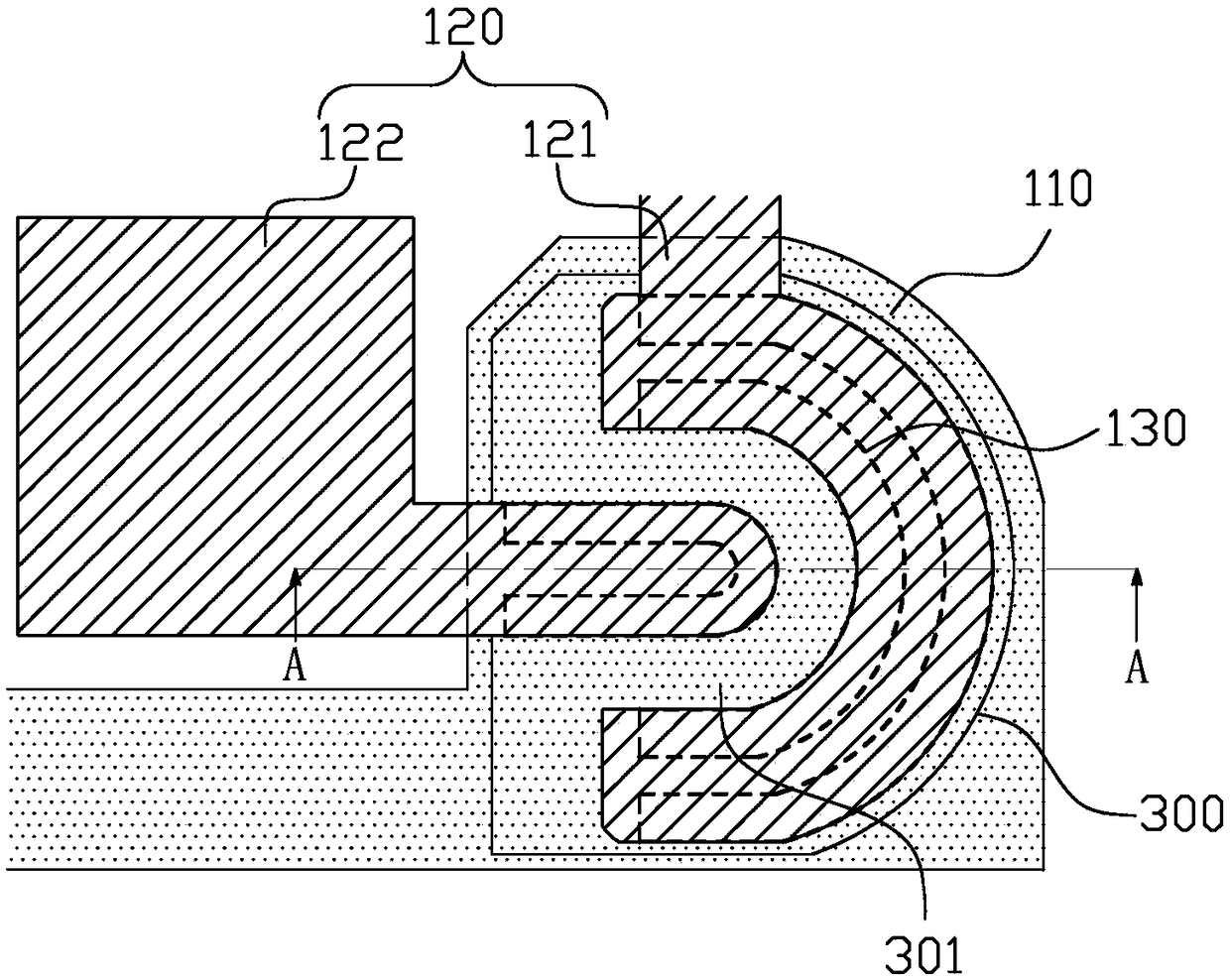
[0059] Please refer to Figure 11 to Figure 14 , The thin film transistor provided by the third embodiment of the present invention includes a gate 110 , a source-drain metal layer 120 and a semiconductor layer 300 disposed on a transparent substrate 100 . Wherein, the gate 110 is arranged on the transparent substrate 100; the gate insulating layer 101 is also provided on the transparent substrate 100 to cover the gate 110; the semiconductor layer 300 is arranged on the gate insulating layer 101 and is located above the gate 110; The drain metal layer 120 is disposed on the semiconductor layer 300, including a source electrode 121 and a drain electrode 122. The source electrode 121 and the drain electrode 122 are separated from each other and are in contact with the semiconductor layer 300. The semiconductor layer 300 is provided with a channel 301, and the channel 301 is provided with between the source 121 and the drain 122 .

[0060] The source 121 is a "U"-shaped or "C"-s...


PUM


Abstract

The invention discloses a thin film transistor. The thin film transistor comprises a gate, a source drain metal layer and a semiconductor layer; the gate is arranged on a transparent substrate; the transparent substrate is also provided with a gate insulating layer for covering the gate; the semiconductor layer is arranged on the gate insulating layer and positioned above the gate; the source drain metal layer is arranged on the semiconductor layer, and comprises a source and a drain; the source and the drain are separated mutually and are in contact with the semiconductor layer; the semiconductor layer has a channel, and the channel is formed between the source and the drain; the gate and the source drain metal layer have an overlapped region in a direction perpendicular to the transparent substrate; and at least one of the gate and the source drain metal layer is provided with a hollow-out structure for reducing the aligned area between the gate and the source drain metal layer. Theinvention also relates to an array substrate and a display apparatus.

Description

technical field [0001] The present invention relates to the technical field of display, in particular to a thin film transistor, an array substrate and a display device. Background technique [0002] Display devices, such as liquid crystal display (liquid crystal display, LCD) have the advantages of good image quality, small size, light weight, low driving voltage, low power consumption, no radiation and relatively low manufacturing cost, and dominate the field of flat panel display. status. A liquid crystal display device includes several parts such as an array substrate, a color filter substrate, and a backlight module. The array substrate includes: a transparent substrate and a plurality of scan lines (Scan Line) and a plurality of data lines (Data Line) formed on the transparent substrate, and a plurality of scan lines and a plurality of data lines intersect each other to form a plurality of pixel units, each Each pixel unit includes a thin film transistor (ThinFilm Tr...

Claims


Application Information

Patent Timeline
IPC IPC(8): H01L29/417H01L29/423H01L29/786H01L27/12
CPCH01L27/1214H01L29/41733H01L29/41775H01L29/42384H01L29/78603
Inventor 杨珊珊魏明贺
Owner KUSN INFOVISION OPTOELECTRONICS
Why Eureka
Try Eureka