

Semiconductor device and manufacturing method thereof
A manufacturing method and semiconductor technology, applied in semiconductor/solid-state device manufacturing, semiconductor devices, electric solid-state devices, etc., can solve the problems of photoresist load effect, reduce the etching precision of device-intensive areas, etc., and achieve the effect of avoiding load effect
Active Publication Date: 2018-10-02
SEMICON MFG INT (SHANGHAI) CORP +1
View PDF2 Cites 2 Cited by
- Summary
- Abstract
- Description
- Claims
- Application Information
AI Technical Summary
Problems solved by technology
[0004] However, there are certain problems in the existing embedded silicon germanium process
Due to the different arrangement densities of devices on the same wafer, the source/drain groove densities of the
Method used
View moreImage
Smart ImageViewing Examples

Examples
 PUM
| Property | Measurement | Unit |
|---|---|---|
| Thickness | aaaaa | aaaaa |
| Thickness | aaaaa | aaaaa |
Abstract
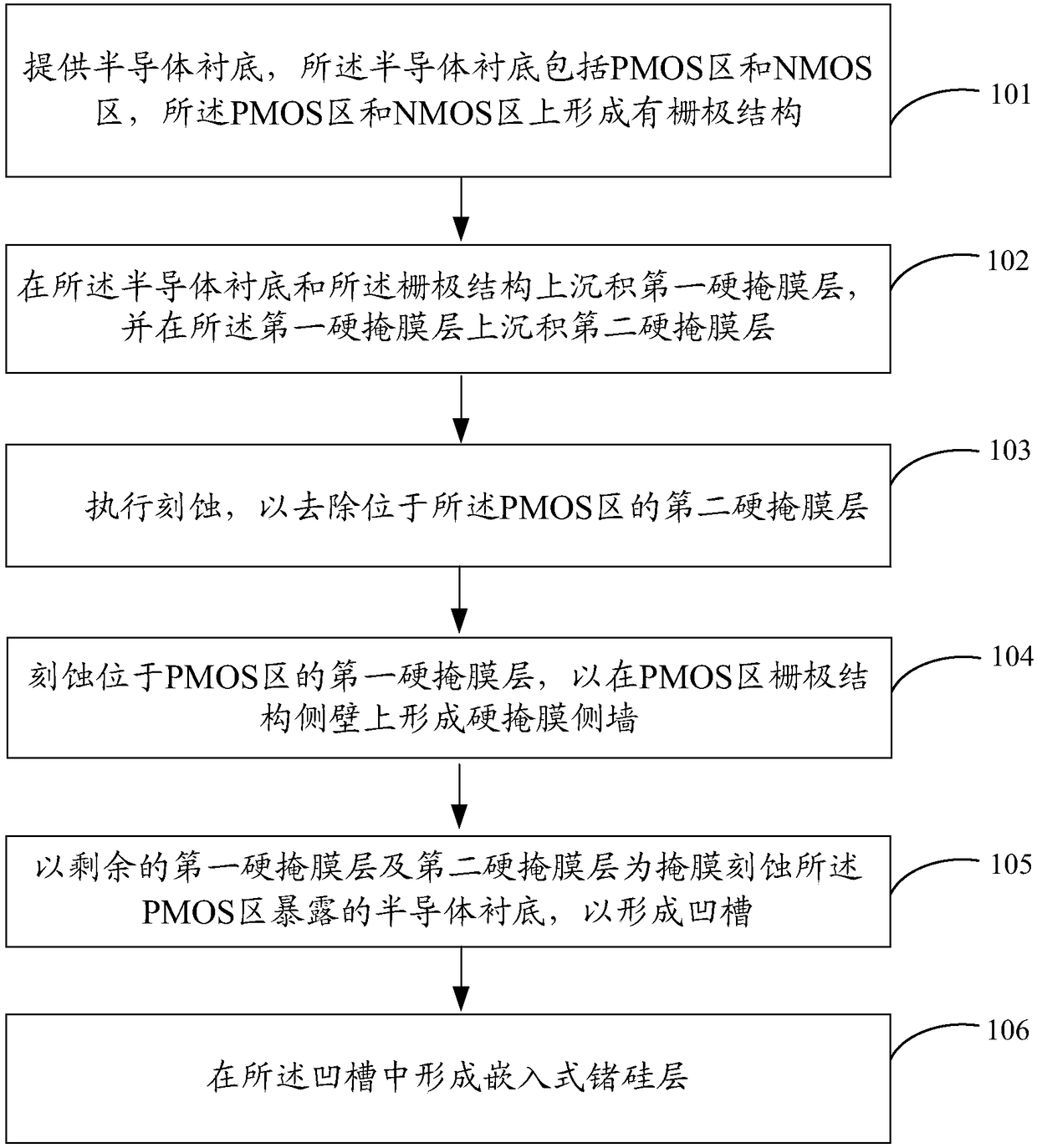
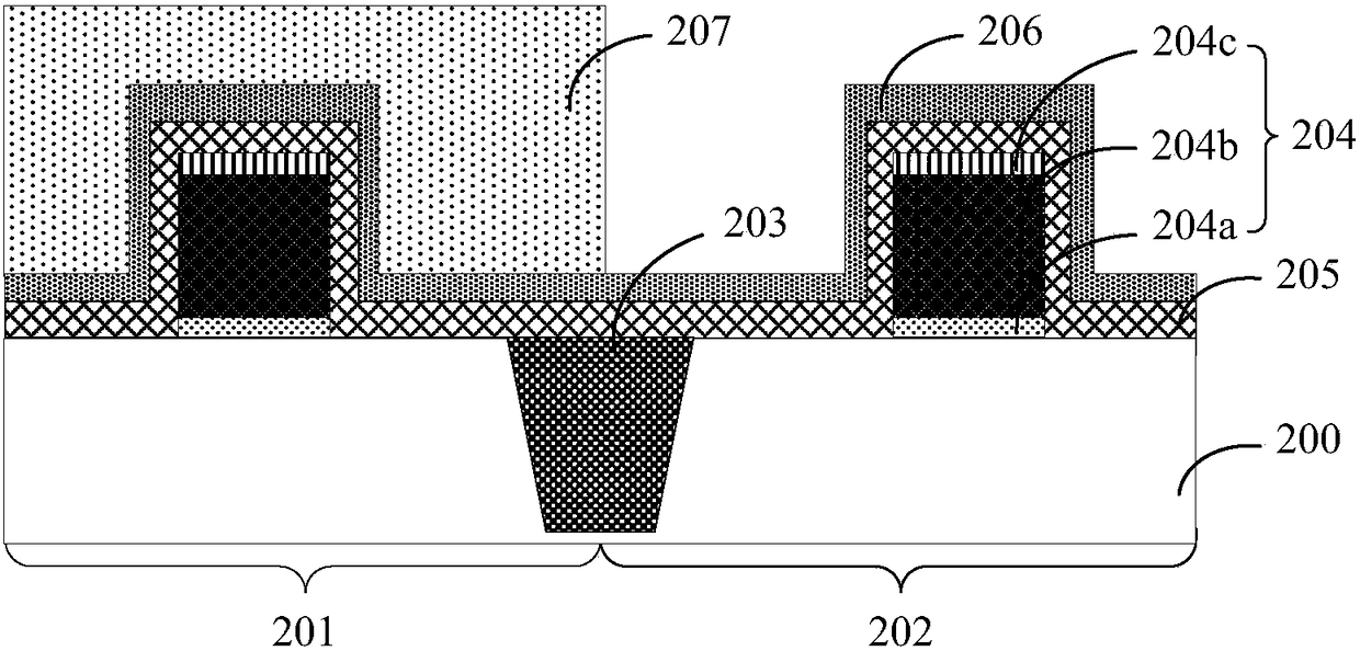
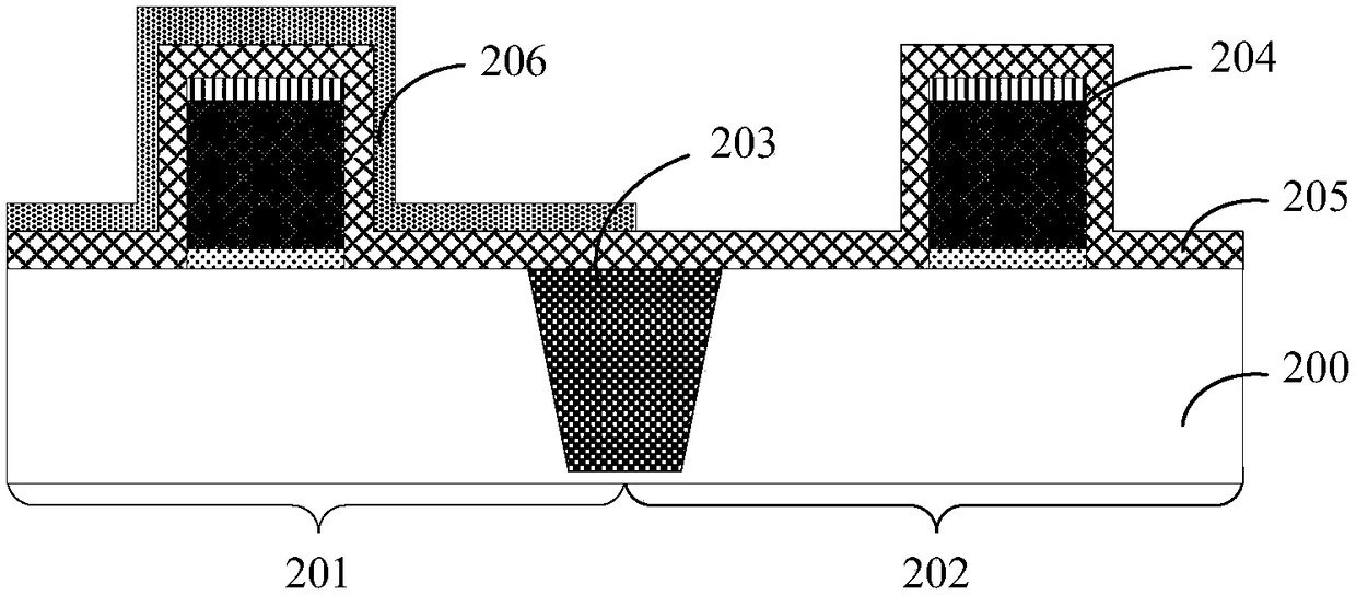
The present invention provides a semiconductor device and a manufacturing method thereof. The manufacturing method includes the following steps that: a semiconductor substrate is provided, wherein thesemiconductor substrate includes a PMOS region and an NMOS region, gate structures being formed on the PMOS region and the NMOS region; a first hard mask layer is deposited on the semiconductor substrate and the gate structures, and a second hard mask layer is deposited on the first hard mask layer; etching is performed so as to remove the second hard mask layer on the PMOS region; the first hardmask layer on the PMOS region is etched, so that a hard mask sidewall can be formed on the sidewall of the gate structure at the PMOS region; with the remaining first hard mask layer and second hardmask layer adopted as a mask, the semiconductor substrate exposed at the PMOS region is etched, so that a groove can be formed; and an embedded germanium silicon layer is formed in the groove. With the manufacturing method of the invention adopted, the load effect of photoresist can be avoided.
Description
Technical field [0001] The invention relates to a semiconductor manufacturing process, in particular to a semiconductor device and a manufacturing method thereof. Background technique [0002] With the continuous development of integrated circuit technology, more devices will be integrated on the chip, and the chip will also adopt faster speeds. With the advancement of these requirements, the geometric dimensions of devices will continue to shrink, and new materials, new technologies and new manufacturing processes will continue to be used in the manufacturing process of chips. At present, the preparation of semiconductor devices has developed to the nanometer level, and the preparation process of conventional devices has gradually matured. [0003] Conventionally, PMOS and NMOS are processed separately in CMOS device manufacturing technology. For example, compressive stress materials are used in the manufacturing method of PMOS devices, and tensile stress materials are used in NM...
Claims
Login to View More Application Information
Patent Timeline
 IPC IPC(8): H01L27/092H01L21/8238
CPCH01L27/0928H01L21/8238
Inventor韩秋华吴端毅
OwnerSEMICON MFG INT (SHANGHAI) CORP