Array substrate, display panel and display device

An array substrate and transistor technology, applied in static indicators, optics, instruments, etc., can solve problems such as low product yield, and achieve the effect of shortening charging time and accurate writing

Active Publication Date: 2018-10-09
BOE TECH GRP CO LTD +1
View PDF10 Cites 10 Cited by
  • Summary
  • Abstract
  • Description
  • Claims
  • Application Information

AI Technical Summary

Problems solved by technology

[0004] Embodiments of the present invention provide an array substrate, a display panel, and a display device, so as to solve the problems in the prior art that fast writing of data signals is realized by changing the material of the active layer, and the product yield is low

Method used


Image

  • Array substrate, display panel and display device
  • Array substrate, display panel and display device
  • Array substrate, display panel and display device

Examples


Embodiment Construction

[0031] In order to make the object, technical solution and advantages of the present invention clearer, the implementation manner of the present invention will be further described in detail below in conjunction with the accompanying drawings.

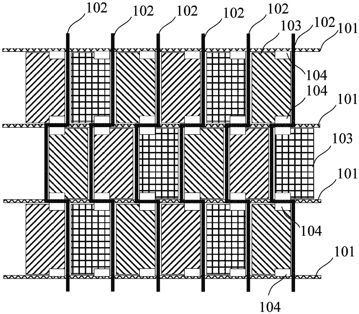
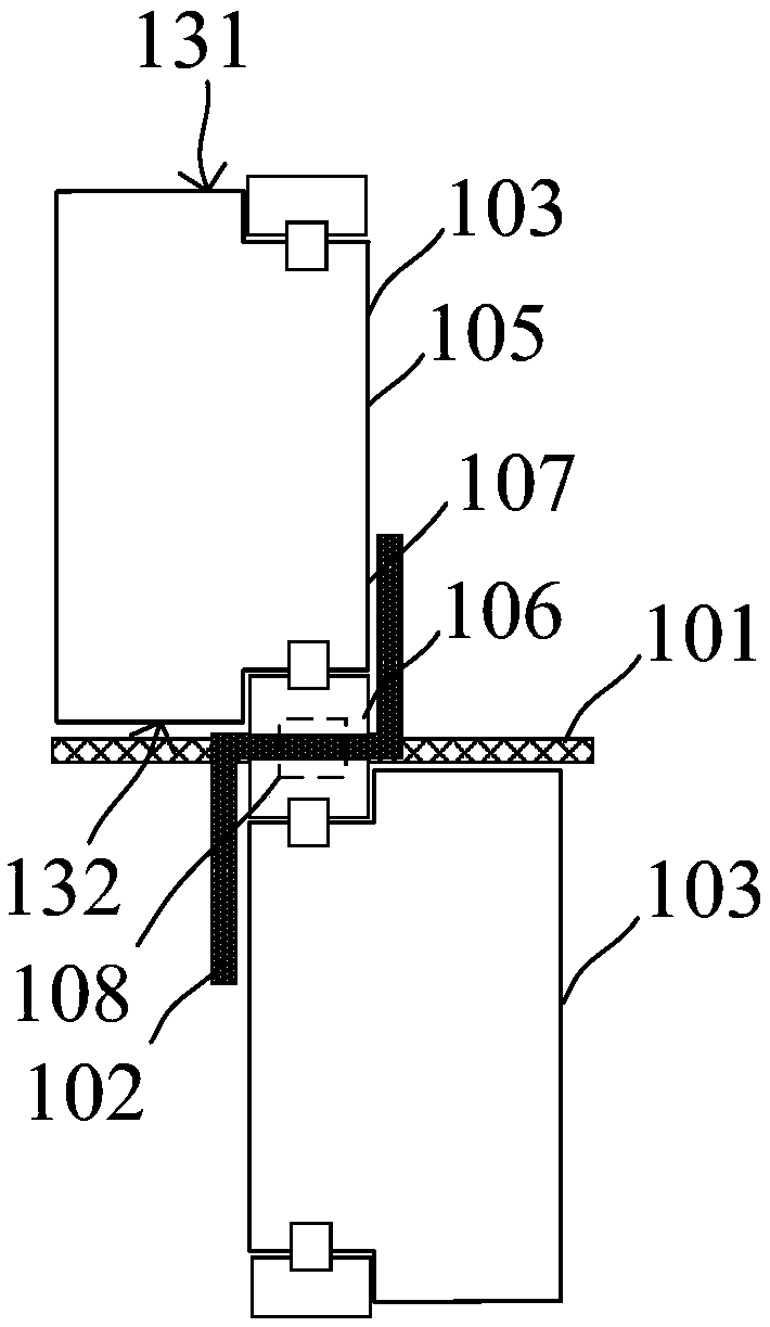
[0032] figure 1 is a schematic structural diagram of an array substrate provided by an embodiment of the present invention, see figure 1 , the array substrate includes: a plurality of gate lines 101 and a plurality of data lines 102, the plurality of gate lines 101 and the plurality of data lines 102 define a plurality of rows of sub-pixel regions 103, each of the sub-pixel regions Two TFTs 104 are arranged in 103 . figure 2 is an enlarged view of the local structure of the array substrate provided by the embodiment of the present invention, see figure 2 , the two TFTs 104 are connected to the pixel electrodes 105 of the sub-pixel regions 103 where they are located.

[0033] see figure 1 , the gates of the two TFTs 104 in the nth...


PUM


Abstract

The invention discloses an array substrate, a display panel and a display device, and belongs to the field of displayers. The array substrate comprises a plurality of grid lines and a plurality of data lines, and multiple rows of sub-pixel areas are defined by the grid lines and the data lines, and the sub-pixel areas are each internally provided with two thin film transistors, wherein the two thin film transistors are connected with pixel electrodes in the sub-pixel area where the two thin film transistors are located respectively, and the grid electrodes of the two thin film transistors in the nth row of sub-pixel area of the multiple rows of sub-pixel areas are connected with the nth grid line and the (n+1)th grid line of the grid lines respectively, n is equal to or smaller than K andequal to or larger than 1, n and K are both an integer, and K is the number of rows of the sub-pixel areas.

Description

technical field [0001] The invention relates to the field of displays, in particular to an array substrate, a display panel and a display device. Background technique [0002] With the development of display technology, the resolution of the display screen is continuously improved, and special display technologies such as 3D display technology and touch display technology are also continuously applied to display products. All of the above development trends require the display screen to be able to write data signals accurately in a shorter period of time. [0003] For a liquid crystal display, the conductivity of a thin film transistor (Thin Film Transistor, TFT) is generally improved by changing the material of the active layer, so as to realize fast writing of data signals. However, when changing the material of the active layer, it is necessary to adjust the manufacturing process of the active layer accordingly, resulting in that the manufacturing process is not mature e...

Claims


Application Information

Patent Timeline
Patent Type & Authority Applications(China)
IPC IPC(8): G02F1/1362
CPCG02F1/13624G02F1/136286G09G3/3677G09G2310/0291G09G2310/0286G09G3/3688H01L27/124H01L27/1251
Inventor 赵斌刘汉青袁旭晨彭勇李慧颖
Owner BOE TECH GRP CO LTD
Why Eureka
Try Eureka