
Charged particle beam device and sample processing method

A technology of charged particle beam and processing method, which is applied in the preparation of test samples, circuits, discharge tubes, etc., can solve the problems such as the inability to produce tiny sample pieces, the inability to accurately grasp the processing end point, and the reduction of the contrast of the processing surface.

Active Publication Date: 2022-03-29
HITACHI HIGH TECH SCI CORP
View PDF13 Cites 0 Cited by
  • Summary
  • Abstract
  • Description
  • Claims
  • Application Information

AI Technical Summary

Problems solved by technology

Therefore, the processing time of the sample becomes longer, and there is also a possibility that a tiny sample piece of the desired shape cannot be produced.
[0011] In addition, when thinning a sample obtained by stacking a plurality of devices in the thickness direction on a semiconductor substrate, and counting the number of devices exposed by processing in order to grasp the processing end point, there is a possibility that the above-mentioned shadow Under the influence of the area, the contrast of the processing surface is reduced, and the number of equipment cannot be accurately counted, so that the processing end point cannot be accurately grasped

Method used


Image

  • Charged particle beam device and sample processing method
  • Charged particle beam device and sample processing method
  • Charged particle beam device and sample processing method

Examples


Embodiment Construction

[0030] Hereinafter, a charged particle beam device and a sample processing method using the charged particle beam device as one embodiment of the present invention will be described with reference to the drawings. In addition, each embodiment shown below is concretely demonstrated for better understanding of the gist of invention, Unless otherwise specified, this invention is not limited. In addition, in order to facilitate understanding of the features of the present invention, the drawings used in the following description may show enlarged main parts for convenience, and the dimensional ratio of each component may not necessarily be the same as the actual one.

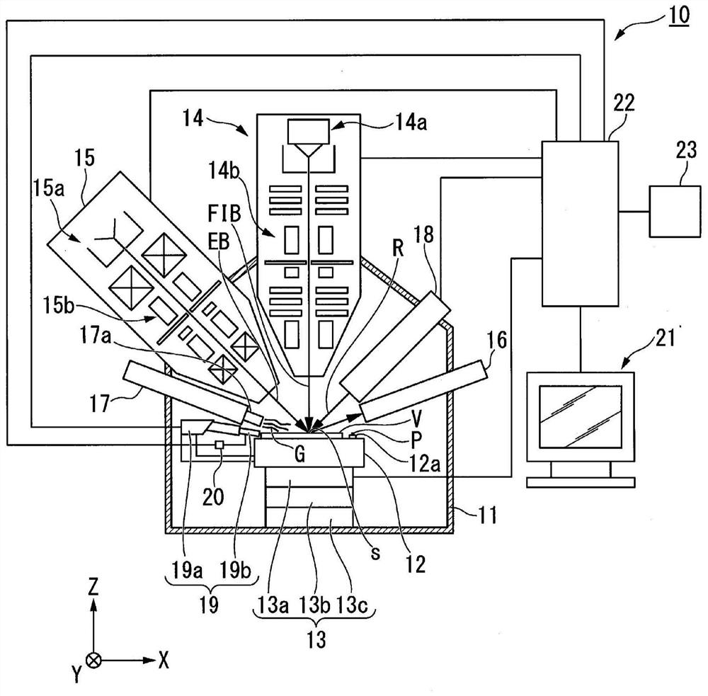
[0031] figure 1 It is a schematic configuration diagram showing a charged particle beam device according to an embodiment of the present invention.

[0032] Such as figure 1 As shown, the charged particle beam device 10 according to the embodiment of the present invention has: a sample chamber 11 capable of mainta...


PUM


Abstract

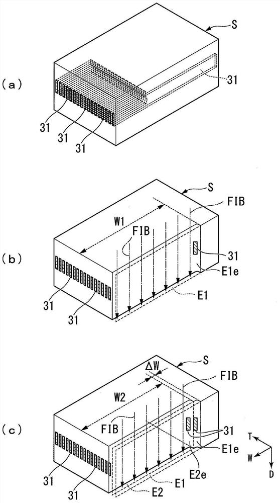
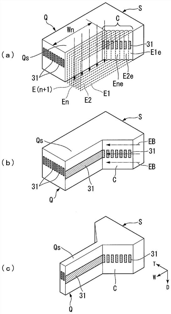
The present invention provides a charged particle beam device and a sample processing method capable of uniformly irradiating a charged particle beam to the entire micro sample piece with reduced sample thickness and clearly grasping the processing end point during processing. The charged particle beam device irradiates a charged particle beam toward a sample to produce a tiny sample piece, and is characterized in that the charged particle beam device has: a charged particle beam lens barrel capable of irradiating a charged particle beam toward the sample; a sample chamber, which accommodates the charged particle beam column; and a sample sheet holder, which can hold the sample. In the case of a sample piece, the portion adjacent to the thinned portion of the micro sample piece forms an inclined portion inclined relative to the thinned portion.

Description

technical field [0001] The present invention relates to a charged particle beam device for processing a sample using a charged particle beam and a sample processing method using the charged particle beam. Background technique [0002] For example, as one method of analyzing or stereoscopically observing the internal structure of a sample such as a semiconductor device, a cross-section processing observation method using a column equipped with a charged particle beam (Focused Ion Beam: FIB) and A charged particle beam recombination device of an electron beam (Electron Beam; EB) column performs FIB-based cross-section forming processing and a scanning electron microscope (Scanning Electron Microscope: SEM) to observe the cross-section (for example, refer to Patent Document 1). [0003] This cross-sectional processing observation method is known as a method of constructing a three-dimensional image by repeatedly performing cross-sectional forming processing by FIB and cross-sec...

Claims


Application Information

Patent Timeline
Patent Type & Authority Patents(China)
IPC IPC(8): H01J37/317G01N1/28
CPCH01J37/317G01N1/28
Inventor 酉川翔太大西毅
Owner HITACHI HIGH TECH SCI CORP
Learn More