Organic electroluminescent device

An electroluminescence device and luminescence technology, applied in circuits, electrical components, electric solid-state devices, etc., can solve the problems of heavy synthesis workload, high research and development costs, and low luminous efficiency, and achieve improved luminous efficiency and expanded color gamut Area, the effect of increasing the color gamut area

Inactive Publication Date: 2018-10-16
YUNGU GUAN TECH CO LTD
View PDF6 Cites 1 Cited by
  • Summary
  • Abstract
  • Description
  • Claims
  • Application Information

AI Technical Summary

Problems solved by technology

[0005] However, the above-mentioned solutions all have their own defects. For example, in the first solution, the design and synthesis of organic light-emitting materials requires a large workload and low yield, and a large number of experimental verifications are required, resulting in high research and development costs; in the second solution, quantum dot technology Although the introduction of LED can improve the color gamut, it is essentially photoluminescence, not electroluminescence, and the luminous efficiency is low

Method used


Image

  • Organic electroluminescent device
  • Organic electroluminescent device
  • Organic electroluminescent device

Examples


Embodiment 1

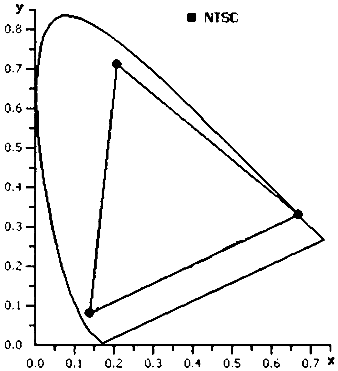
[0079] The embodiment of the present invention provides a specific example of an organic electroluminescence device. The organic electroluminescent device in this embodiment includes monochromatic organic light emitting diodes with three light emitting wavelengths, namely red organic light emitting diodes, green light organic light emitting diodes and blue light organic light emitting diodes. Among them, the three organic light emitting diodes all have a microcavity structure.

[0080] Each organic light-emitting diode includes a first electrode layer, a light-emitting layer and a second electrode layer stacked in sequence, and the light-emitting layer includes a host material and a guest material, the host material includes a thermal activation delay (TADF) material, and the guest material is fluorescent material.

[0081] Wherein, the host material in the light-emitting layer of the red organic light-emitting diode includes a thermally activated delay (TADF) material, and i...

Embodiment 2

[0092] The embodiment of the present invention provides a specific example of an organic electroluminescent device. Its structure is the same as embodiment 1, and the difference with the organic electroluminescent device that embodiment 1 provides is:

[0093] The device of red organic light-emitting diode adopts the traditional host CBP and the phosphorescent guest Ir(piq) 3 , the device of blue-light red-light organic light-emitting diode adopts the traditional host CBP and the fluorescent guest DPVBi.

[0094] The device structure of the red organic light-emitting diode in this embodiment is: ITO (10nm) / Ag (100nm) / ITO (10nm) / CuPc (20nm) / TPD (200nm) / CBP:Ir (piq) 3 (1%,30nm) / TPBi(40nm) / LiF(1nm) / Mg:Ag(20%,15nm) / NPB(60nm)

[0095] The device structure of the blue light organic light emitting diode in the present embodiment is: ITO (10nm) / Ag (100nm) / ITO (10nm) / CuPc (20nm) / TPD (100nm) / CBP:DPVBi (1%, 30nm) / TPBi ( 40nm) / LiF(1nm) / Mg:Ag(20%,15nm) / NPB(60nm)

Embodiment 3

[0097] The embodiment of the present invention provides a specific example of an organic electroluminescent device. Its structure is the same as embodiment 1, and the difference with the organic electroluminescent device that embodiment 1 provides is:

[0098] The mass ratio of the host material and the guest material in the light-emitting layer of the organic light-emitting diode with three light-emitting wavelengths is 95:5.


PUM


Abstract

The invention relates to the technical field of display, and discloses an organic electroluminescent device. The organic electroluminescent device comprises m luminescent units with different luminescent wavelengths; each luminescent unit is a monochromatic light organic luminescent diode or a white light organic luminescent diode provided with a light filter; a luminescent layer inside each organic luminescent diode of a microcavity structure comprises a main body material and an object material, the main body material comprises a thermal activation delay (TADF) material, and the object material is a fluorescent material; and the relation between the microcavity L and the luminescent wavelength lambda of each organic luminescent diode of the microcavity structure meets the relational expression that Li=ni lambda i. Namely, a n-step microcavity effect can be realized in each organic luminescent diode of the microcavity structure, n is a positive integer of greater than or equal to 2, so that a two-step microcavity, a three-step microcavity, a four-step microcavity or a higher-step microcavity can be realized, the effect of the microcavity is strengthened, the spectrum is further narrowed, and then the color gamut area is increased.

Description

technical field [0001] The invention relates to the field of display technology, in particular to an organic electroluminescent device. Background technique [0002] Organic electroluminescence display (English full name Organic Light Emitting Display, referred to as OLED) is an active light-emitting display device, due to its advantages of high contrast, wide viewing angle, low power consumption, thinner volume, etc. It is prepared by a roll to roll process and is easy to realize flexible display, which is one of the most concerned technologies in the current flat panel display technology. [0003] With the continuous development of OLED technology, higher and higher requirements are placed on the performance of display devices. For example, increasing the color gamut, etc. The so-called color gamut is a method of encoding a color, and also refers to the sum of colors that a technical system can produce. figure 1 It is a color coordinate diagram formulated by NTSC (Natio...

Claims


Application Information

Patent Timeline
Patent Type & Authority Applications(China)
IPC IPC(8): H01L51/50H01L51/52H01L27/32
CPCH10K59/30H10K59/38H10K50/12H10K50/852
Inventor 周小康金世遇逄辉何麟李梦真李国孟魏金贝张浩杰田景文李维维李田田
Owner YUNGU GUAN TECH CO LTD
Why Eureka
Try Eureka