Organic electroluminescent device and preparation method thereof

An electroluminescent device and luminescence technology, which is applied in the direction of electric solid-state devices, semiconductor/solid-state device manufacturing, electrical components, etc., can solve the problems of complex process, increase the number of evaporation alignment times, unfavorable mass production, etc., and achieve simplification The effect of technology, improvement of yield rate and cost reduction

Active Publication Date: 2015-05-06
KUNSHAN NEW FLAT PANEL DISPLAY TECH CENT +1
View PDF6 Cites 14 Cited by
  • Summary
  • Abstract
  • Description
  • Claims
  • Application Information

AI Technical Summary

Problems solved by technology

This solution requires the introduction of a precision mask to increase the number of evaporation alignments, and the complex process is not conducive to mass production

Method used


Image

  • Organic electroluminescent device and preparation method thereof
  • Organic electroluminescent device and preparation method thereof
  • Organic electroluminescent device and preparation method thereof

Examples


Embodiment 1

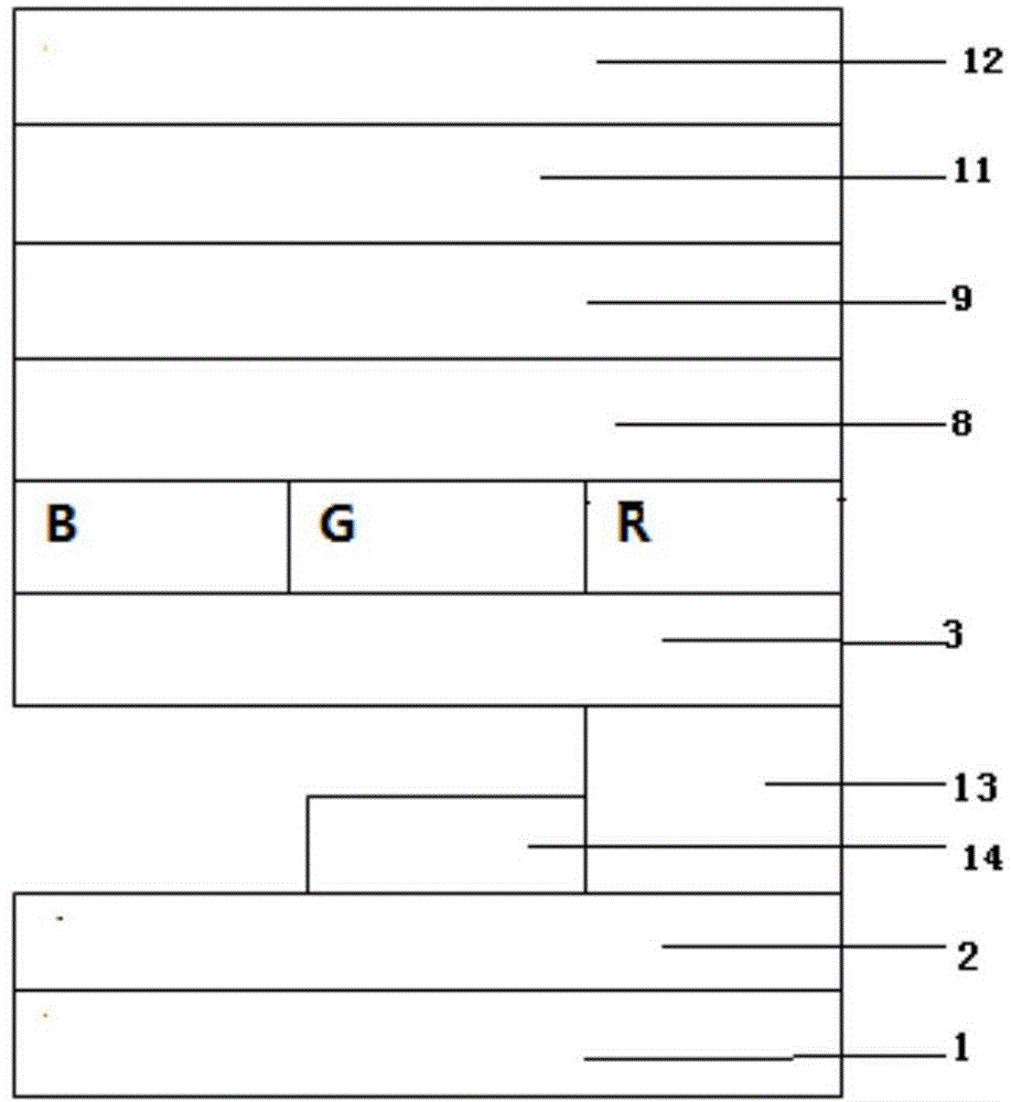
[0041] Such as image 3 As shown, an organic electroluminescent device of the present invention includes a substrate (not shown in the figure), and a first electrode layer 1, several light-emitting unit layers and a second electrode layer sequentially formed on the substrate, Each of the light-emitting unit layers includes a first organic functional layer, a light-emitting material layer, and a second organic functional layer arranged on the first electrode layer 1, and the light-emitting material layer includes a blue light-emitting layer 4 and a green light-emitting layer 5 and a red light-emitting layer 6, the blue light-emitting layer 4 covers the first organic functional layer, the green light-emitting layer 5 is stacked on the blue light-emitting layer 4 and covers part of the blue light-emitting layer 4, the red light-emitting layer A barrier layer 7 is arranged between the light emitting layer 6 and the green light emitting layer 5. The barrier layer 7 described in thi...

Embodiment 2

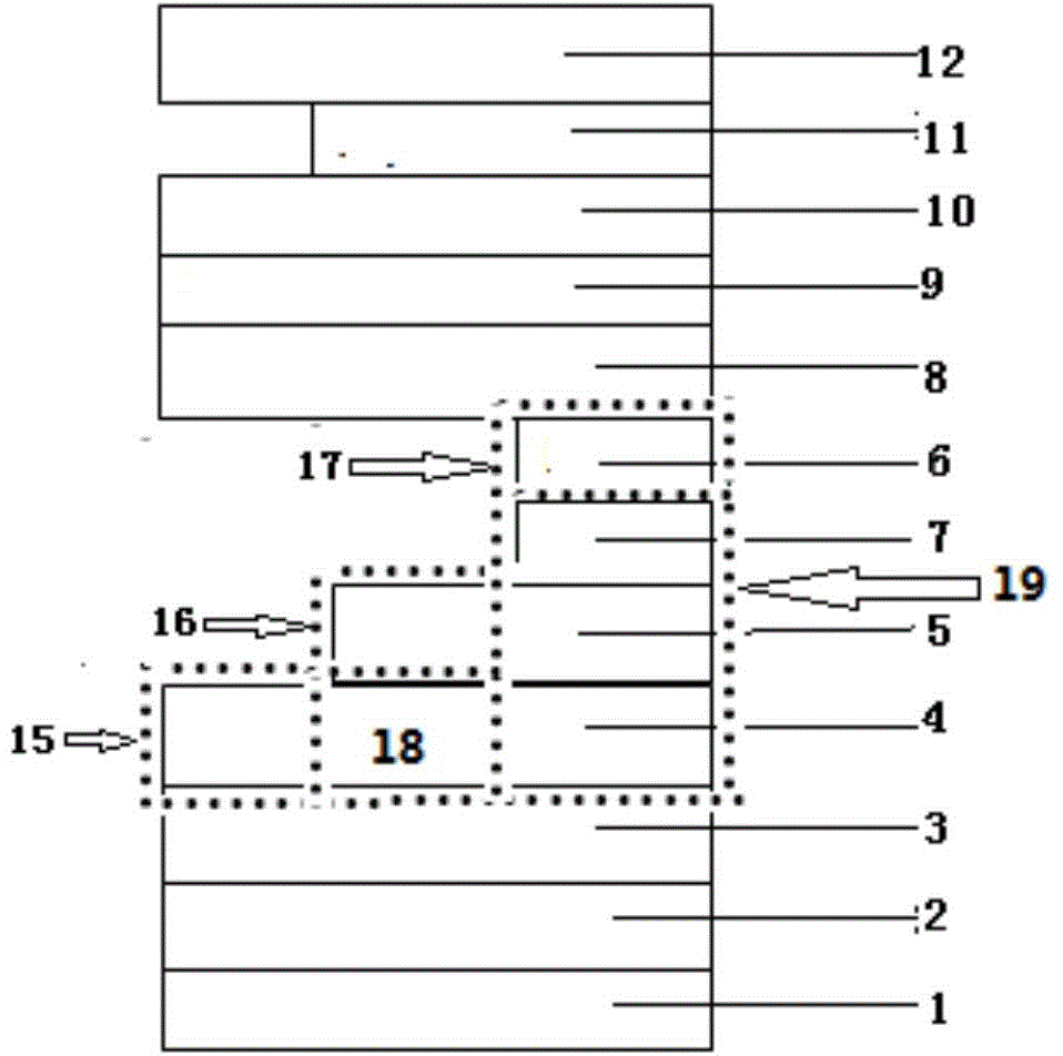
[0057] Figure 4 A kind of organic electroluminescent device of the present invention shown, its structure is the same as embodiment 1, and wherein luminescent material layer comprises blue light emitting layer 4, green light emitting layer 5 and red light emitting layer 6, and red light emitting layer 6 is arranged on On the first organic functional layer, the barrier layer 7 above the red light emitting layer 6 is a hole barrier layer, the green light emitting material layer 5 is above the hole barrier layer, and the blue light emitting material layer 4 is above the green light emitting material layer 5, The blue light emitting layer 4 is covered by the second organic functional layer. Compared with the embodiment, the upper and lower positions of the red light emitting layer 6, the hole blocking layer, the green light emitting layer 5 and the blue light emitting layer 4 are reversed, and the stacking method remains unchanged. The red optical compensation layer 19 is still ...


PUM


Abstract

The invention relates to an organic electroluminescent device. The organic electroluminescent device comprises a substrate, a first electrode layer, a plurality of lighting unit layers and a second electrode layer; the first electrode layer, the plurality of lighting unit layers and the second electrode layer are sequentially formed on the substrate; each lighting unit layer comprises a first organic functional layer, a lighting material layer and a second organic functional layer which are arranged on the first electrode layer; the lighting material layer comprises a blue light lighting layer, a green light lighting layer and a red light lighting layer; the blue light lighting layer is in physical contact with the first organic functional layer or the second organic functional layer; the green light lighting layer is overlapped on the blue light lighting layer and covers part of the blue light lighting layer; a separating layer is arranged between the red light lighting layer and the green light lighting layer; the projection of the red light lighting layer covers part of the green light lighting layer. According to the organic electroluminescent device adopting the structure above, a group of precise mask plates is needed to reach three-color lighting during preparing, and therefore, the yield is increased, the opening rate is increased, and the PPI of a display device is improved.

Description

technical field [0001] The invention relates to the technical field of organic electroluminescent devices, in particular to an organic electroluminescent device with an optical compensation layer, and also relates to a preparation method of the organic electroluminescent device. Background technique [0002] An organic electroluminescent device (OLED) generally includes a plurality of pixels, each pixel consisting of several sub-pixels. One of the currently widely used schemes in small and medium sizes consists of red, green, and blue pixels forming one pixel. In order to obtain higher pixel resolution, the red, green, and blue sub-pixel layers need to use high-precision metal mask evaporation masks in the preparation process. Due to the high precision of the high-precision mask plate, each sub-pixel needs to be adjusted in position, and each adjustment will sacrifice part of the accuracy, thus increasing the cost of the device and limiting the realization of higher resolut...

Claims


Application Information

Patent Timeline
Patent Type & Authority Applications(China)
IPC IPC(8): H01L51/50H01L51/52H01L51/56
CPCH10K50/11H10K2101/10H10K71/00
Inventor 李维维刘嵩
Owner KUNSHAN NEW FLAT PANEL DISPLAY TECH CENT
Why Eureka
Try Eureka