Automobile electronic high-current over-current protection circuit

An overcurrent protection circuit and automotive electronics technology, applied in emergency protection circuit devices, circuit devices, emergency protection devices with automatic disconnection, etc., can solve the problems of slow response time, low selectivity, and inability to realize timely protection of the controller, etc. problems, to achieve fast response time and reduce costs

Pending Publication Date: 2018-10-19
上海拓为汽车技术有限公司
0 Cites 0 Cited by

AI-Extracted Technical Summary

Problems solved by technology

[0002] Conventional over-current protection circuits are mainly aimed at low-current over-current protection, while high-current over-current protection designs mainly use integrated devices, which have high costs. At the same time, there are few existing models of integrated devices and low selectivity.
Some high-cu...

Abstract

The invention relates to an automobile electronic high-current over-current protection circuit comprising a MOS transistor driving circuit, an operational amplifier circuit, and a protection circuit.The input end of the MOS transistor driving circuit is connected with the output end of a driving control module. The output end of the MOS transistor driving circuit is connected with a load module.The input end of the operational amplifier circuit is connected to the output end of the MOS transistor driving circuit. The output end of the operational amplifier circuit is connected to the inputend of the protection circuit. The output end of the protection circuit is connected to the input end of the MOS transistor driving circuit. The automobile electronic high-current over-current protection circuit improves the over-current protection capability of a power circuit and reduces the cost of a controller system.

Application Domain

Emergency protective arrangements for automatic disconnection

Technology Topic

Power circuitsHigh current +6

Image

  • Automobile electronic high-current over-current protection circuit

Examples

  • Experimental program(1)

Example Embodiment

[0012] Below in conjunction with specific embodiment, further illustrate the present invention. It should be understood that these examples are only used to illustrate the present invention and are not intended to limit the scope of the present invention. In addition, it should be understood that after reading the teachings of the present invention, those skilled in the art can make various changes or modifications to the present invention, and these equivalent forms also fall within the scope defined by the appended claims of the present application.
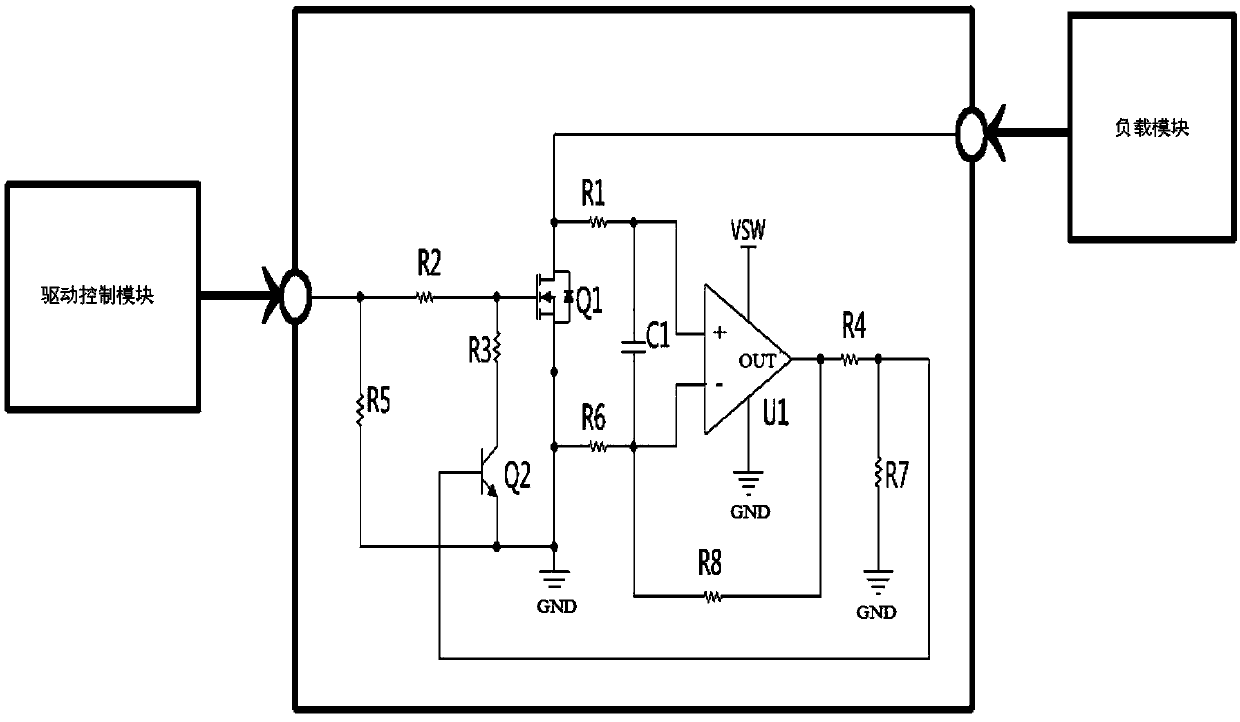
[0013] Embodiments of the present invention relate to a large current overcurrent protection circuit for automotive electronics, such as figure 1 As shown, it includes a MOS tube drive circuit, the input terminal of the MOS tube drive circuit is connected to the output of the drive control module, the output terminal is connected to the load module, and an operational amplifier circuit and a protection circuit are also included. The input terminal of the operational amplifier circuit It is connected with the output end of the MOS transistor drive circuit, the output end is connected with the input end of the protection circuit, and the output end of the protection circuit is connected with the input end of the MOS transistor drive circuit. When working normally, the MOS tube drive circuit works normally, and the operational amplifier circuit and protection circuit do not work; when an overcurrent abnormality occurs, the operational amplifier circuit and protection circuit work, and simultaneously disconnect the MOS tube drive circuit .
[0014] Wherein, the MOS transistor drive circuit includes an N-MOS transistor Q1, a second resistor R2 and a fifth resistor R5, the gate of the N-MOS transistor Q1 is connected to the output of the drive control module through the second resistor R2, the drain is grounded, The source is connected to the load module; one end of the fifth resistor R5 is connected to the output of the drive control module, and the other end is connected to the drain of the N-MOS transistor Q1.
[0015] The operational amplifier circuit includes an operational amplifier U1, a first resistor R1, a sixth resistor R6, an eighth resistor R8, and a capacitor C1; the non-inverting input terminal of the operational amplifier U1 connects with the N-MOS transistor Q1 through the first resistor R1 The source is connected, the inverting input terminal is connected to the drain of the N-MOS transistor Q1 through the sixth resistor R6, and the output terminal is connected to the input terminal of the protection circuit; the non-inverting input terminal of the operational amplifier U1 and the inverting A capacitor C1 is also connected between the phase input ends; one end of the eighth resistor R8 is connected to the output end of the operational amplifier U1, and the other end is connected to the inverting input end of the operational amplifier U1.
[0016] The protection circuit includes an NPN transistor Q2, a third resistor R3, a fourth resistor R4 and a seventh resistor R7; one end of the fourth resistor R4 is connected to the output end of the operational amplifier circuit, and the other end is connected to the output end of the NPN transistor Q2. The base is connected, one end of the seventh resistor R7 is connected to the other end of the fourth resistor R4, and the other end is grounded; the emitter of the NPN transistor Q2 is grounded, and the collector is connected to the MOS tube drive circuit through the third resistor R3 connected to the input.
[0017] The load module in this embodiment can be a high-power device such as a loading motor or a heating wire. When the system is working normally, the drive control module outputs a high level to turn on the N-MOS transistor Q1, and the turned-on N-MOS transistor Q1 The drain of the N-MOS transistor is at a low level, and there is basically no voltage difference between the drain and the source of the N-MOS transistor. The differential voltage between the drain and the source enters the operational amplifier through the input resistors R1 and R6, and the drain-source differential voltage is amplified. The amplified voltage Input to the NPN transistor Q2 through the voltage divider circuit composed of the fourth resistor and the seventh resistor. Since there is basically no voltage difference between the drain and the source, the amplified driving voltage is low level (less than 0.3V) and cannot make the transistor Q2 When it is turned on, the collector of transistor Q2 is still at high level, and the system works normally without abnormality.
[0018] When the system is working, when the port of the load module fails and short-circuits to the power supply, the voltage between the drain and the source of the N-MOS transistor Q1 rises rapidly due to the existence of the Rds resistance of the N-MOS transistor Q1. After the drain-source voltage is amplified by the operational amplifier, it is input to the base of the transistor Q2, the transistor Q2 is quickly turned on, the collector of the transistor Q2 is pulled down to a low level, and the driving N-MOS tube is cut off, thereby realizing a large current overcurrent Protective function.
[0019] In this embodiment, the amplification factor of the operational amplifier circuit can be set by adjusting the resistance values ​​of the first resistor R1 , the sixth resistor R6 and the eighth resistor R8 . The adjustment of the operating voltage threshold of the transistor Q2 can be realized by adjusting the voltage division ratio of the fourth resistor R4 and the seventh resistor R7.
[0020] The main parameters of the overcurrent protection circuit in this embodiment are shown in Table 1:
[0021] Characteristic parameters
[0022] Table 1
[0023] It is not difficult to find that the present invention uses discrete devices to realize the large current overcurrent protection function of the power circuit, reduces the cost of the controller, and at the same time, the protection measure is hardware protection without software intervention, and has the advantage of fast response time.

PUM

no PUM

Description & Claims & Application Information

We can also present the details of the Description, Claims and Application information to help users get a comprehensive understanding of the technical details of the patent, such as background art, summary of invention, brief description of drawings, description of embodiments, and other original content. On the other hand, users can also determine the specific scope of protection of the technology through the list of claims; as well as understand the changes in the life cycle of the technology with the presentation of the patent timeline. Login to view more.

Similar technology patents

Magnetically guided catheter

ActiveUS20100174177A1low costhigh performance
Owner:ST JUDE MEDICAL ATRIAL FIBRILLATION DIV

Head mounted display with eye accommodation

InactiveUS20070097277A1low cost
Owner:UNIV OF CENT FLORIDA RES FOUND INC +1

Method for removing pollutants in sewage

InactiveCN103449680Alow costEasy to prepare
Owner:JIANGSU LV CHUAN ENVIRONMENTAL PROTECTION TECH

Classification and recommendation of technical efficacy words

  • short response time
  • low cost

System and method for transmitting wireless digital service signals via power transmission lines

ActiveUS7929940B1reduce bandwidth requirementlow cost
Owner:NEXTEL COMMUNICATIONS

Plastic waveguide-fed horn antenna

InactiveUS20100214185A1low cost
Owner:RGT UNIV OF CALIFORNIA

System and method for determination of position

InactiveUS20090149202A1low costreduce requirement
Owner:STEELE CHRISTIAN

Adaptive antenna optimization network

InactiveUS6961368B2low costminimal space
Owner:ERICSSON INC
Why Eureka
Try Eureka