Unlock instant, AI-driven research and patent intelligence for your innovation.

Semiconductor device and method for fabricating the same

A technology of semiconductors and devices, applied in the field of semiconductor devices and their manufacturing, can solve the problems such as the influence of the leakage current of refresh characteristics

Active Publication Date: 2018-10-23
SAMSUNG ELECTRONICS CO LTD
View PDF15 Cites 5 Cited by
  • Summary
  • Abstract
  • Description
  • Claims
  • Application Information

AI Technical Summary

Problems solved by technology

For example, the refresh characteristics of DRAM (Dynamic Random Access Memory) can be negatively affected by increased leakage current

Method used


Image

  • Semiconductor device and method for fabricating the same
  • Semiconductor device and method for fabricating the same
  • Semiconductor device and method for fabricating the same

Examples


Embodiment Construction

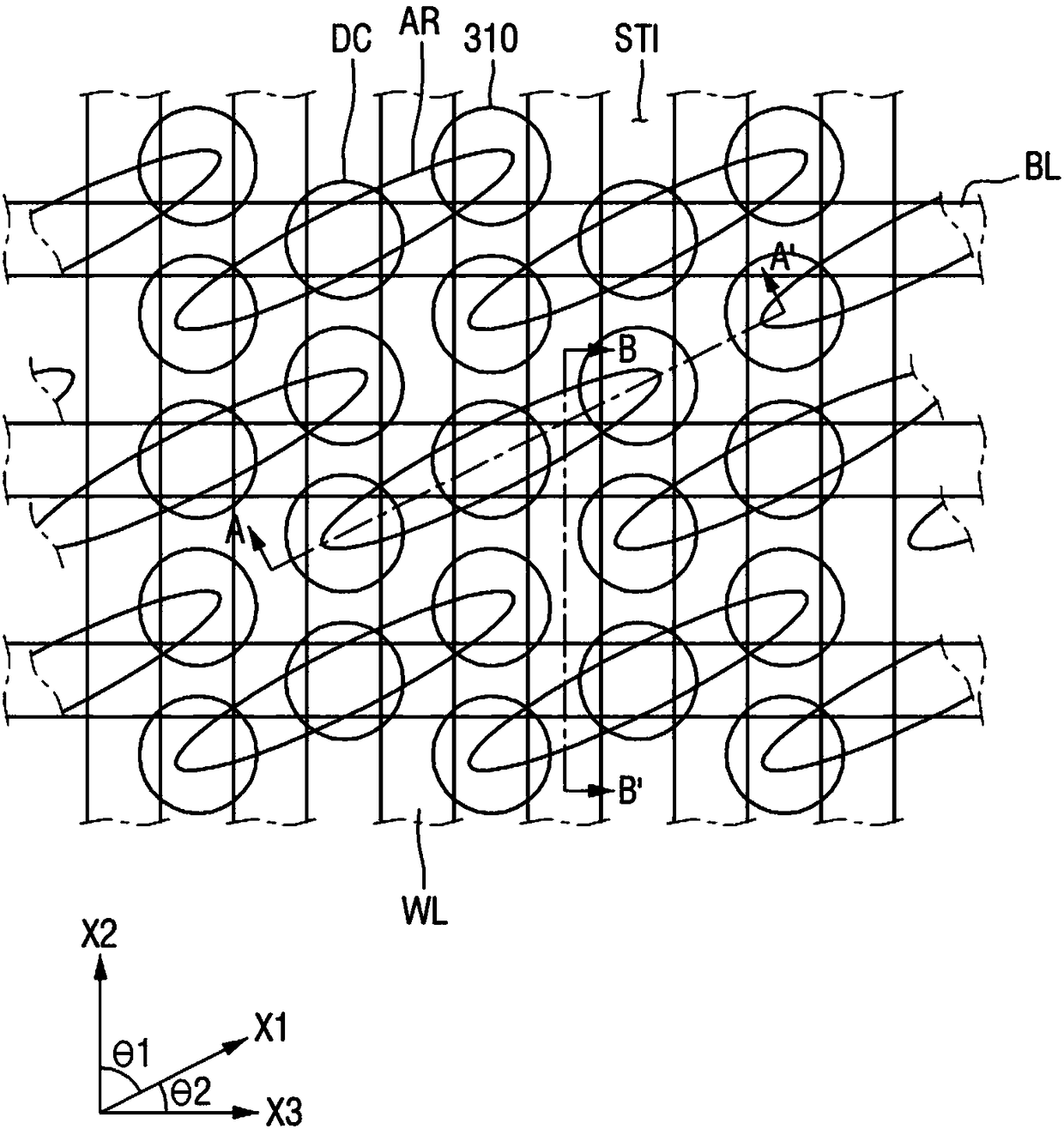
[0014] figure 1 is a layout diagram of a semiconductor device according to some embodiments of the inventive concepts.

[0015] refer to figure 1 , The semiconductor device according to some embodiments of the inventive concept includes a unit active region AR, an element isolation region STI, a word line WL, a bit line BL, a direct contact DC, and a source / drain contact 310 .

[0016] The unit active area AR can be achieved by the substrate ( Figure 2A In 100), an element isolation region (STI; shallow trench isolation) is defined. Specifically, the unit active region AR may extend in the first direction X1.

[0017] The word lines WL may extend in a second direction X2 forming an acute angle with the first direction X1, and the bit lines BL may extend in a third direction X3 forming an acute angle with the first direction.

[0018] Here, the angle in the case of "a specific direction and another specific direction form a predetermined angle" means a smaller angle among ...


PUM


Abstract

A semiconductor device and a method for fabricating the same are provided. The semiconductor device having a substrate can include a lower semiconductor layer, an upper semiconductor layer on the lower semiconductor layer, and a buried insulating layer between the lower semiconductor layer and the upper semiconductor layer. A first trench can be in the upper semiconductor layer having a lowest surface above the buried insulating layer and a first conductive pattern recessed in the first trench. A second trench can be in the lower semiconductor layer, the buried insulating layer, and the uppersemiconductor layer. A second conductive pattern can be in the second trench and a first source / drain region can be in the upper semiconductor layer between the first conductive pattern and the secondconductive pattern.

Description

technical field [0001] The inventive concept relates to semiconductor devices and methods of manufacturing the same. In particular, the inventive concept relates to a semiconductor device including a buried insulating layer and a method of manufacturing the same. Background technique [0002] A buried channel array transistor (BCAT) may include a gate electrode buried in a trench to address short channel effects. [0003] As semiconductor memory devices become more and more highly integrated, the size of each circuit pattern may be reduced to form more semiconductor devices in the same area, which complicates the manufacture of the semiconductor devices. For example, miniaturization of circuit patterns leads to an increase in leakage current. Leakage currents occur in different parts of semiconductor devices. For example, the refresh characteristics of DRAM (Dynamic Random Access Memory) can be negatively affected by increased leakage current. Contents of the invention ...

Claims


Application Information

Patent Timeline
Patent Type & Authority Applications(China)
IPC IPC(8): H01L27/108H01L21/8242
CPCH10B12/315H10B12/053H10B12/485H10B12/0335H10B12/482H01L27/1203H01L21/84H10B12/34H01L29/4236H01L27/1207H10B12/20H10B12/01H01L21/7682
Inventor 赵珉熙金俊秀金熙中安泰玧山田悟李元锡全南镐郑文泳许基宰弘载昊
Owner SAMSUNG ELECTRONICS CO LTD