
Light source circuit board, light source and light source circuit board manufacturing method

A manufacturing method and circuit board technology, applied in the field of lighting, can solve problems such as irregular array arrangement, affecting light efficiency, and difficult control of size consistency, and achieve the effects of ensuring regularity, luminous rate, and consistency

Active Publication Date: 2020-01-03
WUHAN CHINA STAR OPTOELECTRONICS TECH CO LTD
View PDF5 Cites 0 Cited by
  • Summary
  • Abstract
  • Description
  • Claims
  • Application Information

AI Technical Summary

Problems solved by technology

However, in the process of preparing mini-LEDs, due to the difference in processing accuracy and the influence of factors such as the characteristics of the circuit board, it is difficult to control the size consistency of the positive and negative electrodes of the pads on the circuit board. The size of the positive and negative poles of the LED is inconsistent, and the array arrangement will be irregular after the LED pins are connected, which will affect the overall light effect

Method used


Image

  • Light source circuit board, light source and light source circuit board manufacturing method
  • Light source circuit board, light source and light source circuit board manufacturing method
  • Light source circuit board, light source and light source circuit board manufacturing method

Examples


Embodiment Construction

[0029] The following will clearly and completely describe the technical solutions in the embodiments of the present invention with reference to the accompanying drawings in the embodiments of the present invention. Obviously, the described embodiments are only some, not all, embodiments of the present invention. Based on the embodiments of the present invention, all other embodiments obtained by persons of ordinary skill in the art without creative efforts fall within the protection scope of the present invention.

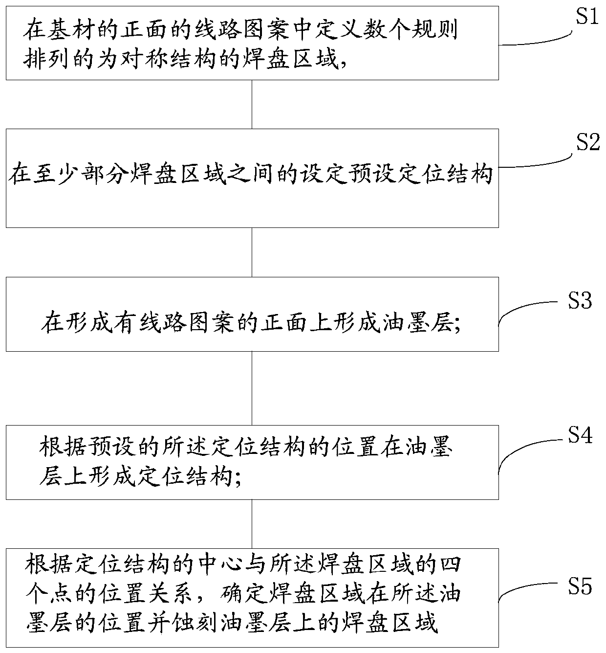
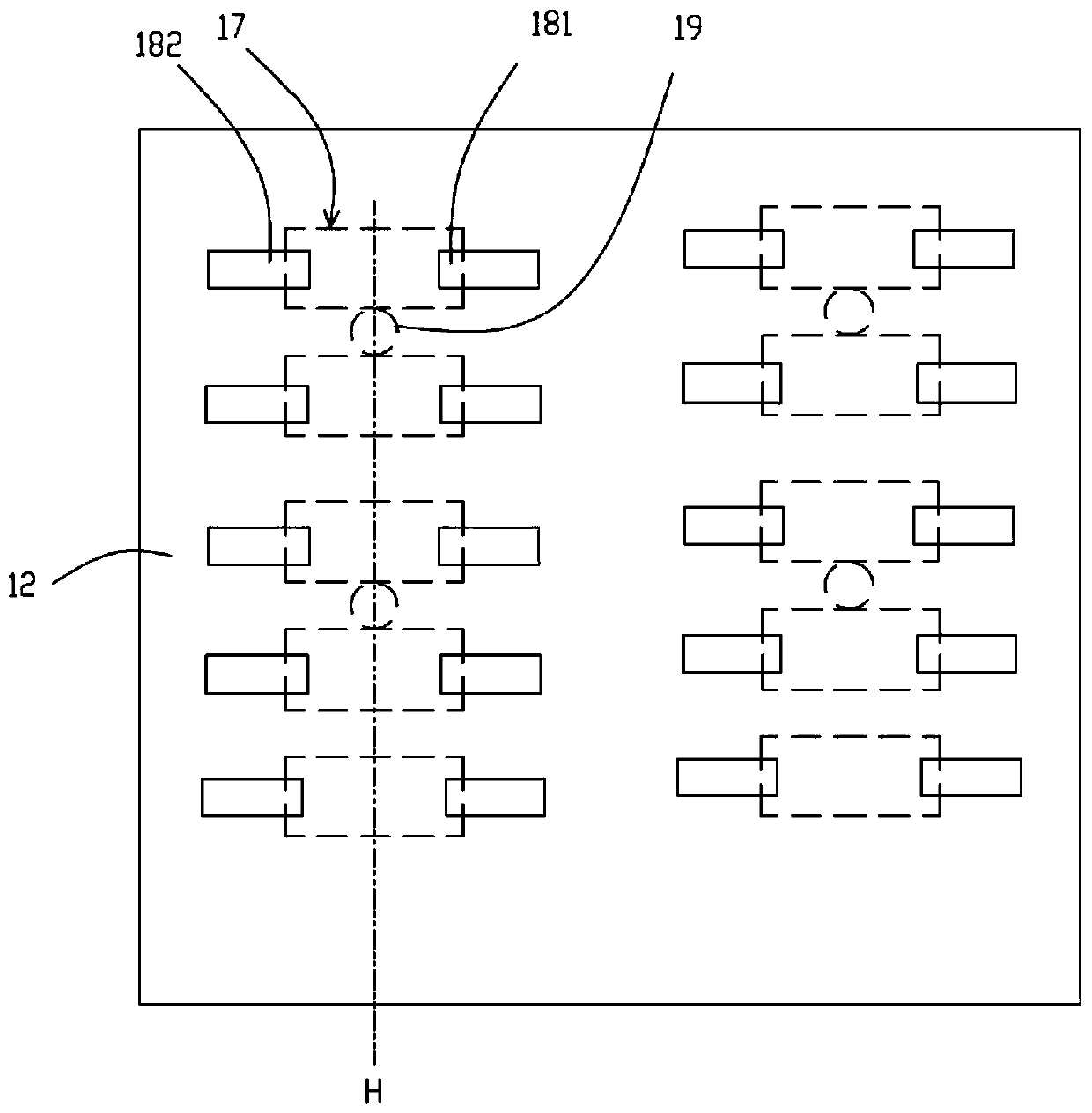
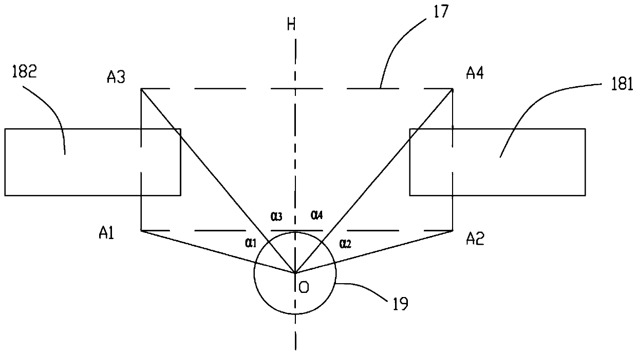
[0030] The invention provides a method for manufacturing a light source circuit board, the method includes, please refer to figure 1 and figure 2 , step S1 , defining several regularly arranged symmetrical pad regions 17 in the circuit pattern on the front surface 111 of the substrate 11 . The pad region 17 is surrounded by a positive electrode 181 and a negative electrode 182 spaced apart from the positive electrode 181 . In this step, the method further includ...


PUM


Abstract

The invention provides a lamp source circuit board production method which comprises the steps of: defining a plurality of bonding pad regions in a circuit pattern of the front side of a base material, which are arranged regularly and are of a symmetrical structure, wherein an anode and a cathode arranged at an interval with the anode are surrounded in each bonding pad region; setting preset positioning structures among at least part of bonding pad regions, wherein each preset positioning structure is positioned at the middle position between two adjacent bonding pad regions in the same column; forming an ink layer on the front side where the circuit pattern is formed; according to the positions of the preset positioning structures, forming positioning structures on the ink layer; and according to a position relationship of the center of each positioning structure and four points of the corresponding bonding pad region, determining a position of the bonding pad region on the ink layerand carrying out etching so as to form a bonding pad including the anode and the cathode which are exposed out of the ink layer.

Description

technical field [0001] The invention relates to the field of lighting technology, in particular to a method for manufacturing a light source circuit board and the light source circuit board. Background technique [0002] For the application of light-emitting diodes, mini-LED (submillimeter light-emitting diode) is currently a hot spot in the market development. It has ultra-thin, high luminous brightness, energy saving, and can be used as a small-sized panel with extremely narrow borders and high dynamic contrast. advantage. However, in the process of preparing mini-LEDs, due to the difference in processing accuracy and the influence of factors such as the characteristics of the circuit board, it is difficult to control the size consistency of the positive and negative electrodes of the pads in the circuit board. The size of the positive and negative poles of the LED is inconsistent, and the array arrangement will be irregular after the LED pins are connected, which will af...

Claims


Application Information

Patent Timeline
Patent Type & Authority Patents(China)
IPC IPC(8): H05K1/02H05K1/11H05K3/24H05K3/30F21V19/00F21Y115/10
CPCF21V19/0015F21Y2115/10H05K1/0271H05K1/111H05K3/24H05K3/303
Inventor 杨勇
Owner WUHAN CHINA STAR OPTOELECTRONICS TECH CO LTD
Learn More