Transparent display panel, display device, light-emitting display device and preparation method

A technology for light-emitting display devices and transparent display panels, which is applied in the manufacture of semiconductor/solid-state devices, semiconductor devices, electric solid-state devices, etc. Effect

Active Publication Date: 2022-02-15
BOE TECH GRP CO LTD
View PDF3 Cites 0 Cited by
  • Summary
  • Abstract
  • Description
  • Claims
  • Application Information

AI Technical Summary

Problems solved by technology

[0004] A main purpose of this application is to solve the problem of unsatisfactory transparency caused by the use of reflective electrodes in existing transparent display products, and to provide a transparent display panel, display device, and light-emitting display that can reduce the use of reflective electrodes and improve transparency. Device and preparation method

Method used


Image

  • Transparent display panel, display device, light-emitting display device and preparation method
  • Transparent display panel, display device, light-emitting display device and preparation method
  • Transparent display panel, display device, light-emitting display device and preparation method

Examples


no. 1 example

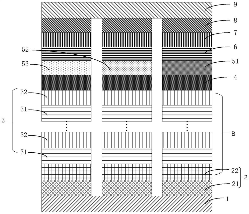
[0035] figure 1 It is a schematic diagram of the layer structure of a light-emitting display device according to the first embodiment. As shown in the figure, this embodiment discloses a light-emitting display device, which mainly includes a substrate 1, a first electrode layer 2, an organic light-emitting layer (3-8) and a second electrode layer 9. The first electrode layer 2 It is arranged on the substrate 1; the light-emitting layer is arranged on the side of the first electrode layer 2 away from the substrate 1, and the hole injection layer 3 in the organic light-emitting layer is adjacent to the first electrode layer 2; the second electrode layer 9 is disposed on the side of the organic light-emitting layer away from the first electrode layer 2; wherein, the hole injection layer 3 and the first electrode layer 2 form a distributed Bragg reflection Mirror structure B, the distributed Bragg reflector structure B includes a plurality of refraction layers, among the pluralit...

no. 2 example

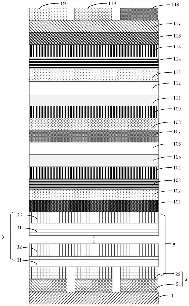
[0058] figure 2 It is a schematic diagram of the layer structure of a light-emitting display device according to the second embodiment. In this embodiment, WOLED (White Organic Light Emitting Diode) + CF (Color Film) is applied to the transparent panel.

[0059] Wherein, in this embodiment, the distributed Bragg mirror structure B is also formed by the hole injection layer 3 and the adjacent first electrode layer 2, and the distributed Bragg mirror structure B includes a plurality of refraction layers, and the plurality of Among the refraction layers, the first refraction layers 31 with the first refraction index and the second refraction layers 32 with the second refraction index are alternately arranged. The electrode reflectivity of the transparent panel can be improved, the brightness and stability of the panel can be improved, the polarization characteristics of the output light of the panel can be improved, and the luminous quality of the panel can be improved. The di...

no. 3 example

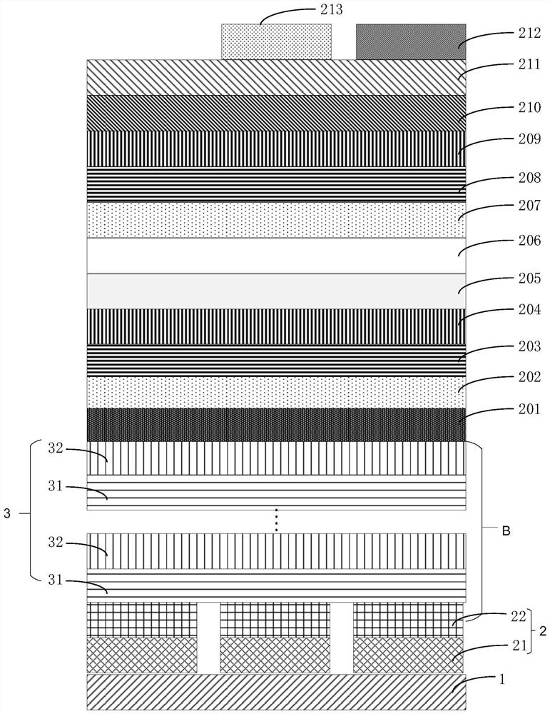
[0065] image 3 It is a schematic diagram of the layer structure of a light-emitting display device according to the third embodiment. In this embodiment, the combination of blue light OLED+quantum dot film is applied to a transparent panel.

[0066] QLED (Quantum Dot Light Emitting Diodes: Quantum Dot Light Emitting Diodes, QLED for short) generally includes a light emitting layer having a plurality of quantum dot nanocrystals. The light emitting layer is sandwiched between the electron transport layer and the hole transport layer. Applying an electric field to a quantum dot LED causes electrons and holes to move into the light-emitting layer. In the light-emitting layer, electrons and holes are trapped in quantum dots and recombine, emitting photons. Compared with organic light-emitting diodes, quantum dot light-emitting diodes have a narrower emission spectrum. Perovskite quantum dots (for example: organic-inorganic hybrid perovskite quantum dots (MAPbX3, MA represents ...


PUM

PropertyMeasurementUnit
thicknessaaaaaaaaaa
thicknessaaaaaaaaaa
refractive indexaaaaaaaaaa

Abstract

The invention relates to the technical field of transparent display, and discloses a transparent display panel, a display device, a light-emitting display device and a preparation method. The light-emitting display device comprises a substrate, a first electrode layer, an organic light-emitting layer and a second electrode layer, wherein the first electrode layer is arranged on the substrate; the light-emitting layer is arranged on the side, away from the substrate, of the first electrode layer, and a hole injection layer in the organic light-emitting layer is adjacent to the first electrode layer; the second electrode layer is arranged on one side, far away from the first electrode layer, of the organic light-emitting layer; wherein the hole injection layer and the first electrode layer form a distributed Bragg reflector structure, the distributed Bragg reflector structure comprises a plurality of refraction layers, the refraction layers with the first refractive index and the refraction layers with the second refractive index in the multiple refraction layers are alternately arranged, and the use of reflecting electrodes can be reduced, so that the transparency is improved.

Description

technical field [0001] The present application relates to the technical field of transparent display, in particular, to a transparent display panel, a display device, a light-emitting display device and a preparation method. Background technique [0002] In recent years, transparent display has gradually become a new display trend. It has great application prospects in many fields such as high-end display, window display, lobby landscape, and new retail. , Smart wearable and other application scenarios are favored, and the development prospect is promising. In the field of transparent display technology development, whether it is traditional LED, OLED or Mini / Micro LED, transparent display products are increasing, and gradually become a new trend in the industry. Among them, OLED panels can emit light without backlight, so there is a strong Transparency and thinness are more suitable for the development of transparent products. [0003] However, because reflective electrod...

Claims


Application Information

Patent Timeline
Patent Type & Authority Applications(China)
IPC IPC(8): H01L51/50H01L51/52H01L51/56H01L27/32
CPCH10K59/00H10K50/17H10K50/805H10K50/852H10K71/00Y02E10/549
Inventor 尤娟娟
Owner BOE TECH GRP CO LTD
Why Eureka
Try Eureka