A kind of preparation method of flip-chip led chip

A LED chip and flip-chip technology, which is applied in semiconductor devices, electrical components, circuits, etc., can solve the problems of insufficient brightness of flip-chip LED chips, prevent diffusion leakage, save manpower and material resources, and improve chip quality.

Active Publication Date: 2020-04-03
LATTICE POWER (JIANGXI) CORP
View PDF4 Cites 0 Cited by
  • Summary
  • Abstract
  • Description
  • Claims
  • Application Information

AI Technical Summary

Problems solved by technology

[0005] Based on the above problems, the object of the present invention is to provide a method for preparing flip-chip LED chips, which effectively solves the technical problem of insufficient brightness of existing flip-chip LED chips.

Method used


Image

  • A kind of preparation method of flip-chip led chip
  • A kind of preparation method of flip-chip led chip
  • A kind of preparation method of flip-chip led chip

Examples


Embodiment Construction

[0028] In order to make the technical problems, technical solutions and beneficial effects solved by the present invention clearer, the present invention will be further described in detail below in conjunction with the embodiments.

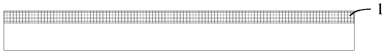
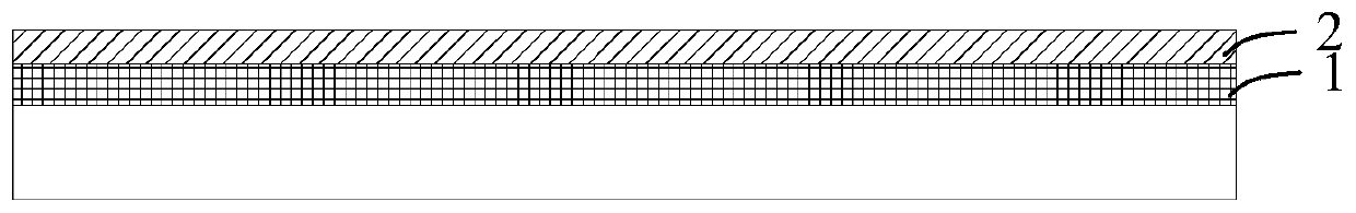
[0029] 1. Epitaxial wafers after Mg activation (such as figure 1 As shown, on the substrate and the epitaxial layer 1), use plasma to grow the first protective layer 2 under certain conditions (such as: 100-400 ° C, etc.), as a passivation layer and isolation film, to protect / block the high reflection metal ,Such as figure 2 shown. In an example, the first protection layer can be grown by using materials such as SiO2, SiON, SiN, etc., and the thickness of the growth can be 1000-20000 angstroms.

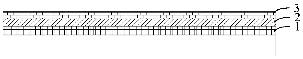
[0030] 2. On the epitaxial wafer with the first protective layer 2 grown, sputter and evaporate one or more layers of metal / metal alloy as the first alloy layer 3, such as image 3 shown. Afterwards, the sputtered and evaporated metal / metal alloy i...


PUM

PropertyMeasurementUnit
thicknessaaaaaaaaaa

Abstract

The invention provides a method for preparing a flip-chip LED chip, comprising: S1 preparing an epitaxial wafer; S2 preparing a first protective layer on the epitaxial wafer; S3 preparing a first alloy layer on the surface of the first protective layer; S4 etching the first alloy layer according to a preset image. A protective layer and the first alloy layer; S5 sequentially prepares a highly reflective metal layer and a second alloy layer on the surface of the epitaxial wafer in the etching area, wherein the thickness of the highly reflective alloy layer is the same as that of the first protective layer; S6 does not etch in the etching step S4 area until the epitaxial layer is exposed; S7 sequentially prepares the second protective layer, electrodes, third protective layer and pads on the surface of the second alloy layer to complete the preparation of the flip-chip LED chip. The "light-absorbing" metal at the edge of its highly reflective metal layer is very narrow or even absent, greatly improving the brightness of flip-chip LED chips.

Description

technical field [0001] The invention belongs to the field of semiconductors, and in particular relates to a method for preparing a flip-chip LED chip. Background technique [0002] LED (Light Emitting Diode, Light Emitting Diode) is a solid-state semiconductor device capable of converting electrical energy into visible light, which can directly convert electrical energy into light energy. As a new type of lighting source material, it is widely used in various fields. Due to the problems of poor heat dissipation, uneven current distribution of transparent electrodes, and light blocking of surface electrode pads and leads in traditional formal LEDs, more and more manufacturers and engineers are committed to seeking new technologies for preparing LED chips, and flip chip technology has come into play. And born. [0003] At present, flip-chip technology continues to mature in the field of LEDs, and its applications are becoming more and more extensive, such as in Ball Grid Arr...

Claims


Application Information

Patent Timeline
Patent Type & Authority Patents(China)
IPC IPC(8): H01L33/40H01L33/46
CPCH01L33/405H01L33/46H01L2933/0016
Inventor 金力彭翔赵汉民汤松龄
Owner LATTICE POWER (JIANGXI) CORP
Why Eureka
Try Eureka