Chip binding mechanism and chip packaging machine

A chip and bonding technology, applied in the direction of electrical components, semiconductor/solid-state device manufacturing, circuits, etc., can solve problems such as difficulties and achieve the effect of improving the efficiency of chip bonding

Pending Publication Date: 2018-11-06
大连佳峰自动化股份有限公司
View PDF0 Cites 6 Cited by
  • Summary
  • Abstract
  • Description
  • Claims
  • Application Information

AI Technical Summary

Problems solved by technology

At present, most placement machines use a single-head binding mechanism. The UPH (number of patches per ho

Method used


Image

  • Chip binding mechanism and chip packaging machine
  • Chip binding mechanism and chip packaging machine
  • Chip binding mechanism and chip packaging machine

Examples


Embodiment Construction

[0025] The following will clearly and completely describe the technical solutions in the embodiments of the present invention with reference to the accompanying drawings in the embodiments of the present invention. Obviously, the described embodiments are only some, not all, embodiments of the present invention. Based on the embodiments of the present invention, all other embodiments obtained by persons of ordinary skill in the art without making creative efforts belong to the protection scope of the present invention.

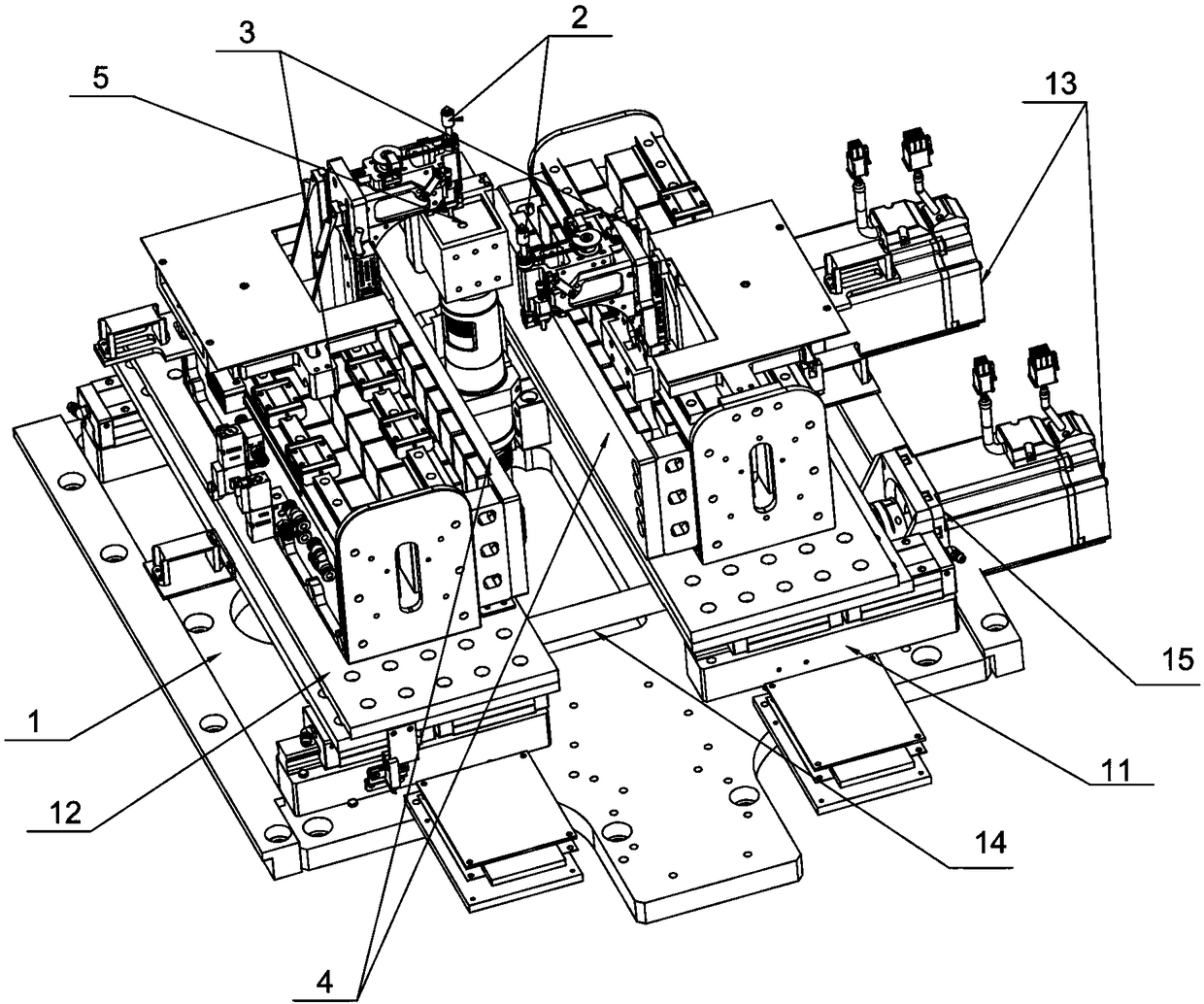
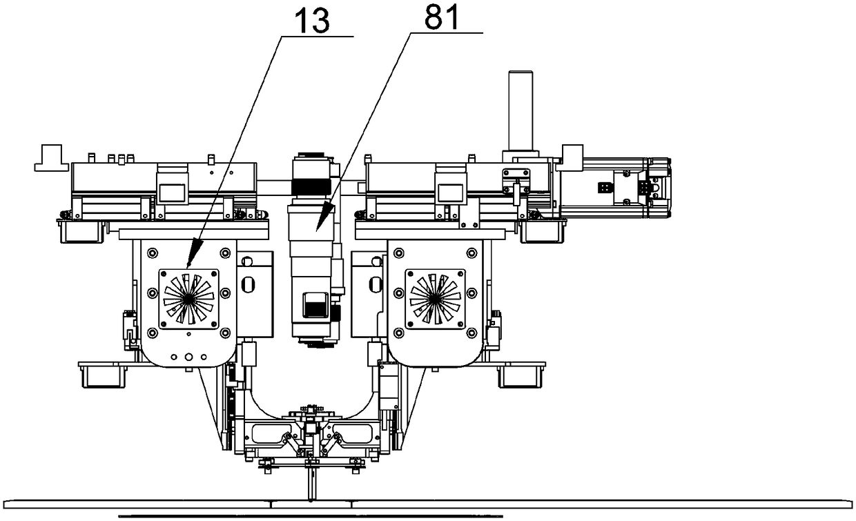
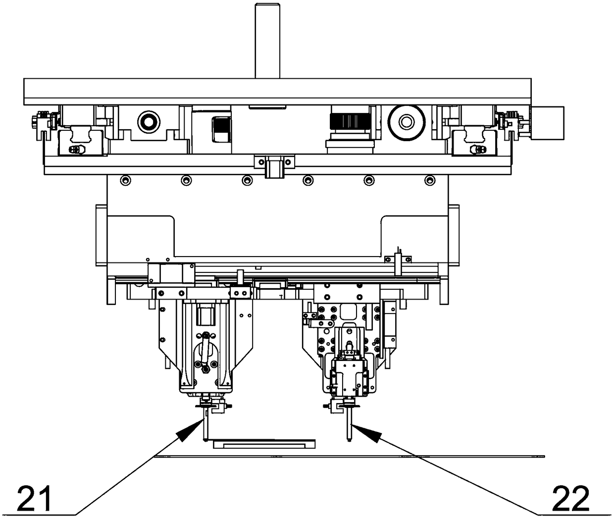
[0026] The purpose of the present invention is to provide a chip bonding mechanism and a chip packaging machine to solve the above-mentioned problems in the prior art, use two bonding heads to bond a row of chips at the same time, increase the chip speed, and reduce the manufacturing cost of the mechanism.

[0027] In order to make the above objects, features and advantages of the present invention more comprehensible, the present invention will be further desc...


PUM


Abstract

The invention discloses a chip binding mechanism, the chip binding mechanism comprises a platform, two lateral rails parallel to a lateral direction of the platform are arranged on the platform, eachlateral rail is connected with a lateral sliding block through sliding connection, and a lateral driving component is used for driving one lateral sliding block to slide on the lateral rail in a reciprocating mode; a binding head longitudinal rail parallel to a longitudinal direction of the platform is arranged on each lateral sliding block, one binding head longitudinal sliding block is connectedon each binding head longitudinal rail through sliding connection, and a longitudinal driving component is used for driving the binding head longitudinal sliding block to slide on the binding head longitudinal rail in the reciprocating mode; a vertical rail in a vertical direction is arranged on each binding head longitudinal sliding block, and a vertical driving component is used for driving onevertical sliding block to slide on the vertical rail in the reciprocating mode; and each vertical sliding block is fixedly connected with one binding head. According to the chip binding mechanism andthe chip packaging machine of the chip binding mechanism, two binding heads are used for binding a series of chips at the same time, thus, chip speed is promoted, and mechanism manufacturing cost isreduced.

Description

technical field [0001] The invention relates to the technical field of semiconductor packaging equipment, in particular to a chip binding mechanism and a chip packaging machine. Background technique [0002] The chip binding mechanism is a mechanism that picks up the chip from the carrier (wafer or waffle tray, etc.) in various placement machines and places the chip on the binding position on the lead frame or substrate. At present, most placement machines use a single-head binding mechanism. The UPH (number of patches per hour) of the equipment has reached the bottleneck. It is very difficult to increase the UPH of the equipment. Contents of the invention [0003] The purpose of the present invention is to provide a chip bonding mechanism and a chip packaging machine to solve the above-mentioned problems in the prior art, use two bonding heads to bond a row of chips at the same time, increase the chip speed, and reduce the manufacturing cost of the mechanism. [0004] To...

Claims


Application Information

Patent Timeline
IPC IPC(8): H01L21/67
CPCH01L21/67011H01L21/67121
Inventor 粱吉来孙永军张飞王云峰
Owner 大连佳峰自动化股份有限公司
Why Eureka
Try Eureka