Terminal for semiconductor power device

A technology for power devices and semiconductors, which is applied to semiconductor devices, electrical components, circuits, etc., and can solve the problems of reducing chip terminal characteristics and large electric field peaks.

Pending Publication Date: 2018-11-06
盛廷微电子(深圳)有限公司
View PDF0 Cites 2 Cited by
  • Summary
  • Abstract
  • Description
  • Claims
  • Application Information

AI Technical Summary

Problems solved by technology

[0003] However, since the field limiting ring and the field plate of the terminal of the IGBT are ring structures, that is, the four corners of the chip are all curved, so there is a curvat

Method used


Image

  • Terminal for semiconductor power device
  • Terminal for semiconductor power device
  • Terminal for semiconductor power device

Examples


Embodiment Construction

[0024] The following descriptions of the various embodiments refer to the accompanying drawings to illustrate specific embodiments in which the present invention can be practiced. The directional terms mentioned in the present invention, such as "up", "down", "front", "back", "left", "right", "inside", "outside", "side", etc., are for reference only The orientation of the attached schema. Therefore, the directional terms used are used to illustrate and understand the present invention, but not to limit the present invention. In the figures, structurally similar units are denoted by the same reference numerals.

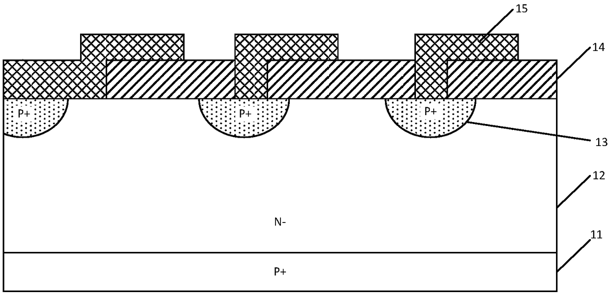
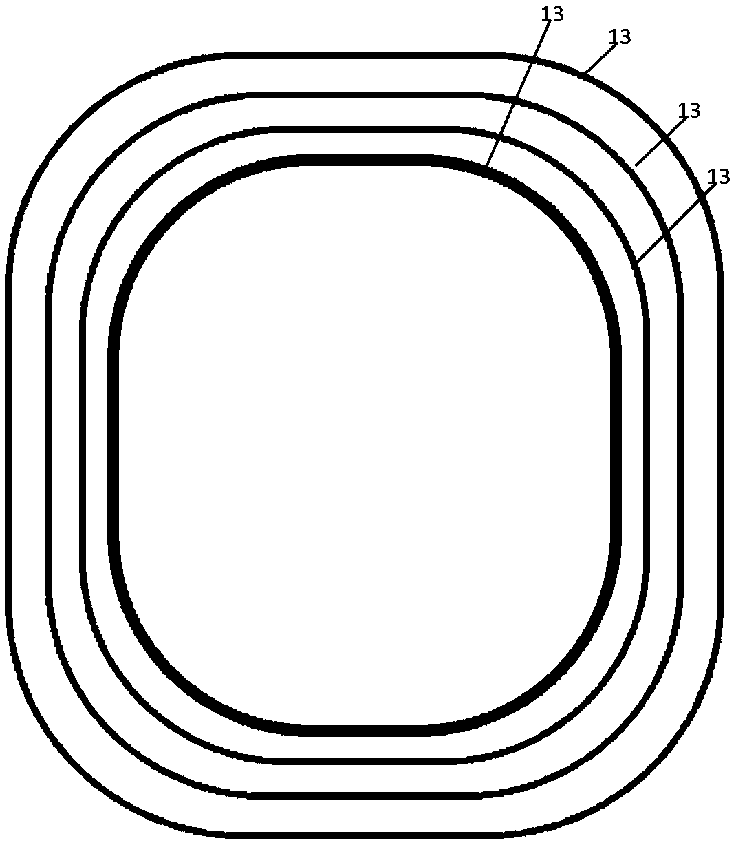
[0025] Such as figure 1 As shown, the existing terminals for semiconductor power devices include a collector 11, a base region 12 (that is, a substrate), a plurality of field limiting rings 13, and a dielectric layer 14 arranged between the field limiting rings 13 and the field plates 15 As well as the field plate 15, the field confinement ring 13 is formed by two d...


PUM


Abstract

The invention provides a terminal for a semiconductor power device. The terminal for the semiconductor power device comprises a collector electrode, a base region, a plurality of annular field limiting rings and a plurality of metal field plates corresponding to the field limiting rings, wherein the field limiting rings are arranged at intervals; the intervals between two adjacent field limiting rings are equal; the field limiting rings comprise a plurality of main bending parts and a plurality of main straight parts; the main bending parts are positioned between two adjacent main straight parts; the widths of the main bending parts decrease gradually along the middles of the main bending parts to two sides; the widths of the main bending parts of the field limiting rings are larger than the widths of the main straight parts of the corresponding field limiting rings; and the widths of the main bending parts increase gradually from sides close to geometric centers of the field limitingrings to sides far away from the geometric centers of the field limiting rings. Through adoption of the terminal for the semiconductor power device provided by the invention, the electric field spikesat corners can be reduced, and the stability and reliability of the semiconductor power device are enhanced.

Description

【Technical field】 [0001] The invention relates to the technical field of semiconductor devices, in particular to a terminal for semiconductor power devices. 【Background technique】 [0002] The terminal (Insulated Gate Bipolar Transistor, IGBT) used for semiconductor power devices is a composite fully-controlled voltage-driven power semiconductor device composed of BJT (bipolar transistor) and MOS (insulated gate field effect transistor). It has the advantages of unipolar devices and bipolar devices, and its driving circuit is simple, the power consumption and cost of the control circuit are low, and the on-state voltage is low. It has become one of the mainstream power semiconductor devices. [0003] However, since the field limiting ring and the field plate of the terminal of the IGBT are ring structures, that is, the four corners of the chip are all curved, so there is a curvature effect at the four corners of the chip. Due to the curvature effect, the electric field at th...

Claims


Application Information

Patent Timeline
IPC IPC(8): H01L29/06H01L29/40H01L29/739
CPCH01L29/0619H01L29/0684H01L29/404H01L29/407H01L29/7393
Inventor 缪志平
Owner 盛廷微电子(深圳)有限公司
Why Eureka
Try Eureka