Quantum dot light-emitting diode and preparation method thereof and display panel
A quantum dot light-emitting and diode technology, applied in semiconductor/solid-state device manufacturing, electrical components, circuits, etc., can solve the problems of increasing device fabrication cost, difficult to control layer thickness, poor repeatability, etc., to improve device luminous efficiency, reduce Electron transport or injection, the effect of saving the cost of preparation
- Summary
- Abstract
- Description
- Claims
- Application Information
AI Technical Summary
Problems solved by technology
Method used
Image

Examples
Embodiment 1
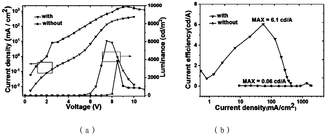
[0047] This embodiment provides a quantum dot light-emitting diode. By doping one or more substances that can capture carriers in the electron transport layer, the electron injection of the trans-structure quantum dot light-emitting diode can be effectively improved, and the electron transport can be improved. rate, to obtain a higher device luminous efficiency.
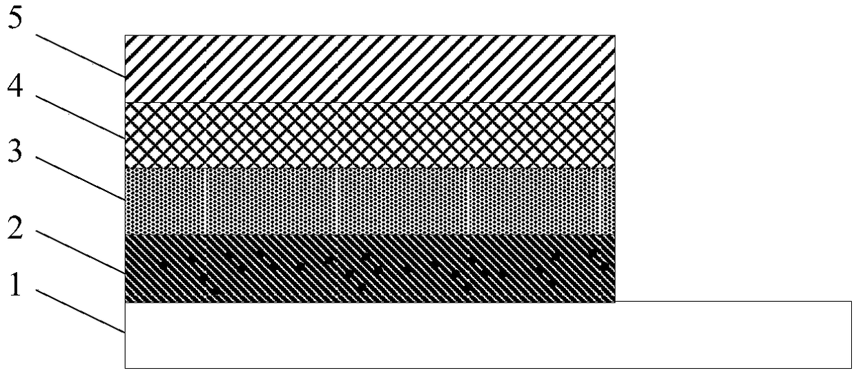
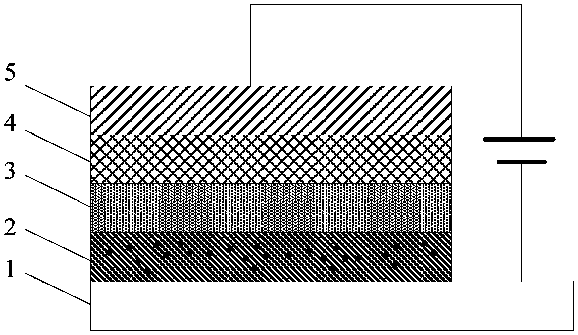
[0048] Such as figure 1 As shown, the quantum dot light-emitting diode is a top-emitting (Top-emitting) inverted structure (Inverted Structure) or trans-structure, including sequentially stacked cathode 1, electron transport layer 2, light-emitting layer 3, hole transport layer 4 and anode 5. Correspondingly, the preparation method of the quantum dot light-emitting diode includes the steps of forming a cathode 1, an electron transport layer 2, a light emitting layer 3, a hole transport layer 4 and an anode 5, and the electron transport layer 2 includes a substance capable of capturing carriers , substances capable ...
Embodiment 2
[0057] This embodiment provides a quantum dot light-emitting diode. By doping one or more substances that can capture carriers in the electron transport layer, a top-emitting quantum dot light-emitting diode can be prepared by the full solution method, which can effectively improve the trans The electronic injection of the structural quantum dot light-emitting diode improves the electron transport rate and obtains a higher device luminous efficiency.
[0058] The structure reference of the quantum dot light-emitting diode in this embodiment figure 1 , the process of preparing the quantum dot light-emitting diode by the whole solution method is as follows:
[0059] Step S1): Perform pretreatment on the substrate as the cathode: the pretreatment includes cleaning and plasma treatment.
[0060] Cleaning: The substrate is made of ITO or FTO. Since there are usually some dust and organic matter on the surface of the newly purchased or manufactured substrate, it is necessary to per...
Embodiment 3
[0090] This embodiment provides a quantum dot light-emitting diode. By doping one or more substances that can capture carriers in the electron transport layer 2, a top-emitting quantum dot light-emitting diode can be prepared by the full solution method, which can effectively improve the reflection efficiency. The electronic injection of the quantum dot light-emitting diode with the formula structure improves the electron transmission rate and obtains a higher device luminous efficiency.
[0091] The difference between this example and Example 2 lies in the difference in the method for preparing the anode 5. In Example 2, the PEDOT:PSS film is obtained by spin coating. In this example, the PEDOT:PSS film is transferred to the device through the PDMS intermediate medium by transfer printing technology. .
[0092] For the preparation method of the quantum dot light-emitting diode of this embodiment, the pretreatment of the substrate and the pretreatment of the materials of each ...
PUM
| Property | Measurement | Unit |
|---|---|---|
| Thickness | aaaaa | aaaaa |
Abstract
Description
Claims
Application Information
 - R&D Engineer
- R&D Manager
- IP Professional
- Industry Leading Data Capabilities
- Powerful AI technology
- Patent DNA Extraction
Browse by: Latest US Patents, China's latest patents, Technical Efficacy Thesaurus, Application Domain, Technology Topic.
© 2024 PatSnap. All rights reserved.Legal|Privacy policy|Modern Slavery Act Transparency Statement|Sitemap