Light emitting device and light source imaging system

A light-emitting device and imaging system technology, which is applied in the direction of light source, lighting device, light source fixation, etc., can solve the problems of large light-emitting angle, failure to collect LED outgoing light, unfavorable high-brightness light source, etc., and achieve the effect of high brightness

Inactive Publication Date: 2018-11-13
DONGGUAN INST OF OPTO ELECTRONICS PEKING UNIV
View PDF10 Cites 0 Cited by
  • Summary
  • Abstract
  • Description
  • Claims
  • Application Information

AI Technical Summary

Problems solved by technology

However, since the LED has a certain light-emitting area and the light-emitting angle of the LED is relatively large (generally 90 degrees), the collimator lens cannot collect all the outgoing light of the LED, and can only collect the outgoing light within a certain sending angle.
[0003] Moreover, the collimation effect of a collimating lens on the outgoing light of the LED is poor, so a collimating lens group is used to work together to collimate the outgoing light of an LED. The collimating lens group generally includes 2 to 3 lens
[0004] However, the design of multiple lenses is difficult to maintain the etendue of the LED outgoing beam. Generally, after being collimated by the collimating lens group, the etendue of the outgoing beam will increase by three to five times, which is not conducive to obtaining a high-brightness light source.

Method used


Image

  • Light emitting device and light source imaging system
  • Light emitting device and light source imaging system
  • Light emitting device and light source imaging system

Examples


Embodiment Construction

[0025] In order to further understand the features, technical means, and specific objectives and functions achieved by the present invention, the present invention will be further described in detail below in conjunction with the accompanying drawings and specific embodiments.

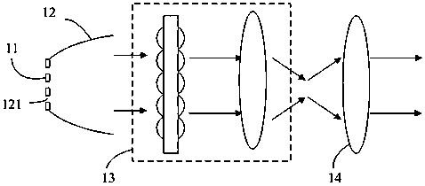
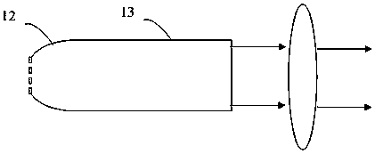
[0026] as attached figure 1 As shown, a light emitting device is packaged with a light source, and the light source includes a light emitting element array 11 and a compound parabolic concentrator 12 with a light entrance.

[0027] The light-emitting element array is arranged at the light entrance of the compound parabolic light collector, so that the compound parabolic light collector collects the light beams from the light-emitting element array, and the sum of the light-emitting areas of each light-emitting element in the light-emitting element array is greater than or equal to that of the compound parabolic light collector. 50% of the area of ​​the light entrance of the optical device. The light-e...


PUM


Abstract

The invention discloses a light emitting device and a light source imaging system. The light emitting device comprises light sources; the light sources comprise light emitting element arrays and composite paraboloid light collectors with light inlets; the light emitting element arrays are arranged at the light inlets of the composite paraboloid light collectors, and thus the composite paraboloid light collectors collect light beams from the light emitting element arrays; and the sum of the light emitting area of all light emitting elements in the light emitting element arrays is greater than or equal to 50% of the area of the light inlets of the composite paraboloid light collectors. According to the light emitting device and the light source imaging system, the light beams with the high brightness can be emerged, and the light out efficiency is improved.

Description

technical field [0001] The invention belongs to the technical field of display and illumination, in particular to a light emitting device and a light source imaging system. Background technique [0002] In the LED array in the light source device of the stage light, each LED corresponds to a collimating lens, so that the collimating lens can collimate the emitted light of the LED. However, since the LED has a certain light-emitting area and the light-emitting angle of the LED is relatively large (generally 90 degrees), the collimator lens cannot collect all the outgoing light of the LED, but can only collect the outgoing light within a certain sending angle. [0003] Moreover, the collimation effect of a collimating lens on the outgoing light of the LED is poor, so a collimating lens group is used to work together to collimate the outgoing light of an LED. The collimating lens group generally includes 2 to 3 lens. [0004] However, the design of multiple lenses is difficul...

Claims


Application Information

Patent Timeline
Patent Type & Authority Applications(China)
IPC IPC(8): F21K9/20F21V19/00F21K9/68F21K9/69F21K9/64F21K9/60F21K9/61F21Y115/10F21Y113/13
Inventor 欧阳晓希郑小平童玉珍李顺峰卢洪王琦张国义
Owner DONGGUAN INST OF OPTO ELECTRONICS PEKING UNIV
Why Eureka
Try Eureka