A system and method for detecting bubbles and crease defects in straight lines of flexible IC substrates
A defect detection and detection method technology, applied in the field of defect detection, can solve the problems of detection algorithms or few papers, and achieve the effect of avoiding false positives of defects
- Summary
- Abstract
- Description
- Claims
- Application Information
AI Technical Summary
Problems solved by technology
Method used
Image
Examples
Embodiment
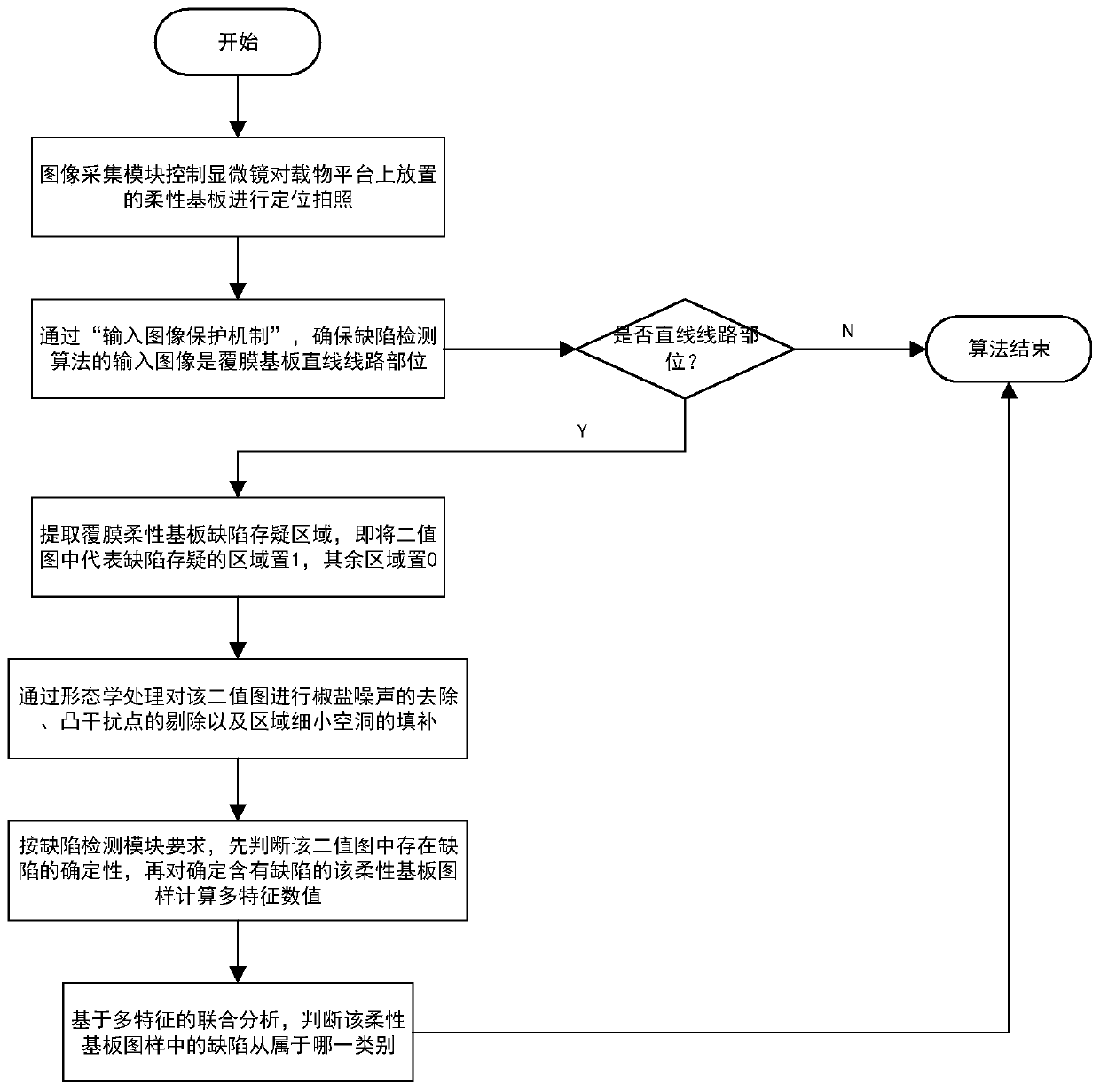
[0058] Such as figure 1 As shown, a method for detecting bubbles and crease defects in a straight line of a flexible IC substrate in this embodiment includes the following steps:
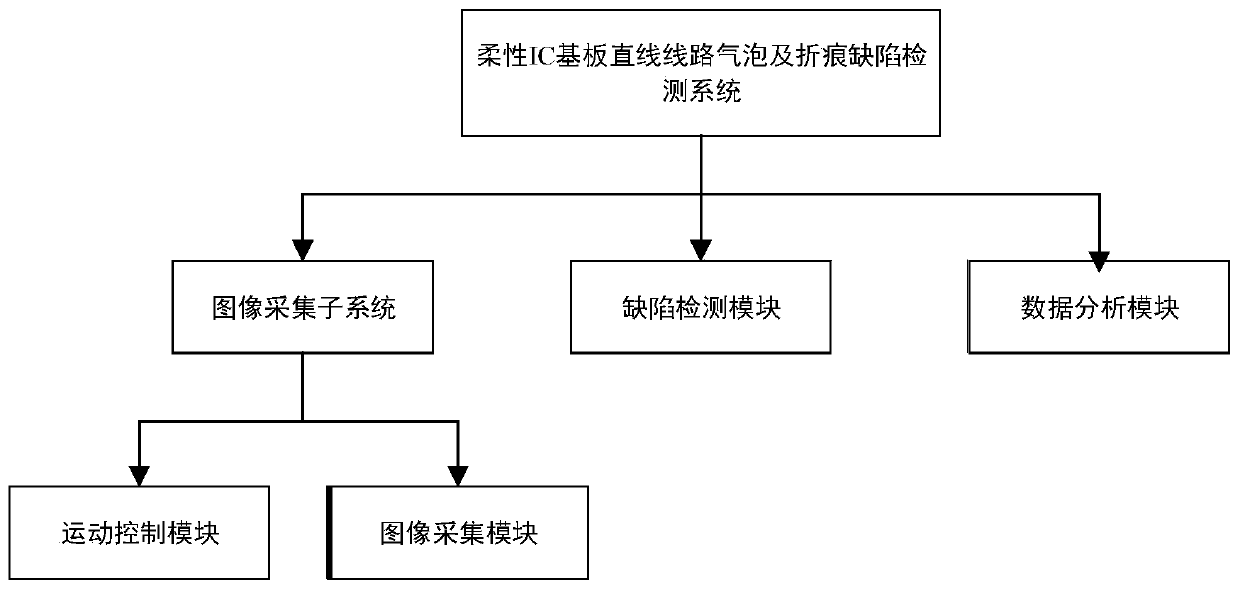
[0059] S1. The image acquisition subsystem controls the microscope to position and take pictures of the flexible substrate placed on the loading platform, and the target position is the area where the film-coated straight line is located;
[0060] S2. Through the "input image protection mechanism", ensure that the input image of the defect detection algorithm is the line part of the film-coated flexible substrate, otherwise a pop-up window will warn and exit the algorithm process;
[0061] S3. Extracting the area with doubtful defects in the film-coated flexible substrate, that is, setting the area representing doubtful defects in the binary image to 1, and setting the remaining areas to 0;
[0062] S4. Remove salt and pepper noise, remove convex interference points, and fill small holes in the bin...
PUM
 Abstract
Description
Claims
Application Information


