

Method for preparing mask plate
A mask and mask technology, applied in the semiconductor field, can solve the problem of low wafer publishing efficiency, and achieve the effects of improving publishing efficiency, reducing the number of false positives, and reducing the time required for inspection
- Summary
- Abstract
- Description
- Claims
- Application Information
AI Technical Summary
Problems solved by technology
Method used
Image


Examples
Embodiment Construction
[0030] The preparation method of the reticle proposed by the present invention will be further described in detail below with reference to the accompanying drawings and specific embodiments. It should be noted that all the drawings are in a very simplified form and use imprecise scales, and are only used to facilitate and clearly assist the purpose of illustrating the embodiments of the present invention. In addition, the structures shown in the drawings are often a part of the actual structures. In particular, each drawing needs to display different emphases, and sometimes uses different scales.
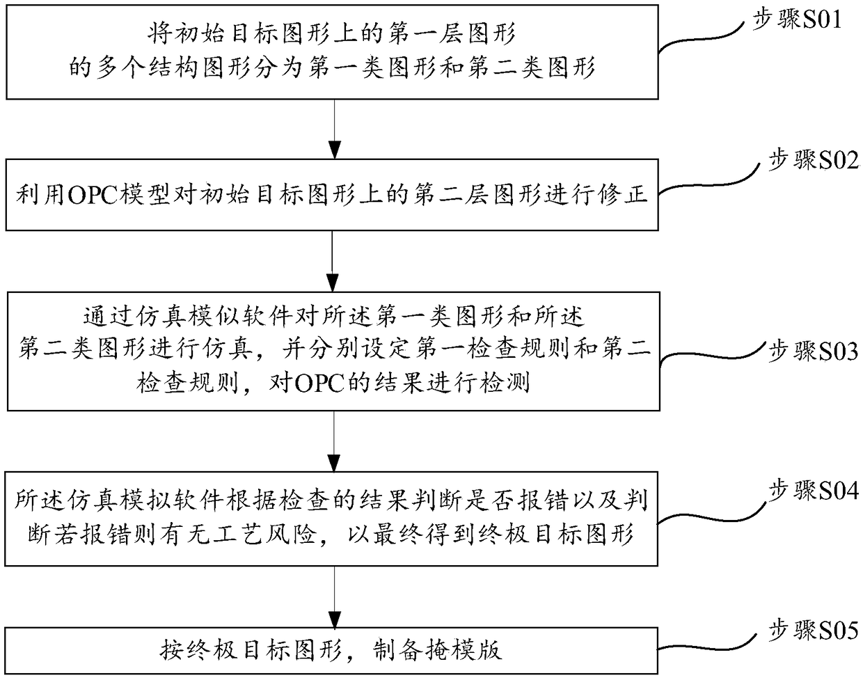
[0031] Such as figure 1 As shown, the embodiment of the present invention provides a method for preparing a mask.
[0032] First, step S01 is executed to provide an initial target graphic, the initial target graphic includes a first layer graphic and a second layer graphic, the first layer graphic includes a plurality of structural graphics, a plurality of the structures are arran...
PUM
 Abstract
Description
Claims
Application Information