Operating method for P channel flash memory unit
An operation method and flash memory cell technology, which are applied in the field of integrated circuit manufacturing, can solve the problem that the performance of P-channel flash memory needs to be improved, etc., and achieve the effects of area shrinkage, device area reduction, and high impact ionization rate.
- Summary
- Abstract
- Description
- Claims
- Application Information
AI Technical Summary
Problems solved by technology
Method used
Image

Examples
Embodiment Construction
[0029] The specific implementation manner of the present invention will be described in more detail below with reference to schematic diagrams. It should be noted that, the accompanying drawings are all in a very simplified form and in inaccurate scales, and are only used to facilitate and clearly assist the purpose of explaining the embodiments of the present invention.
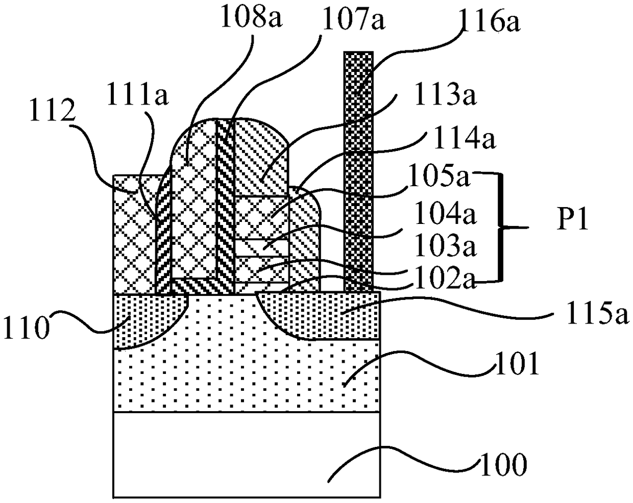
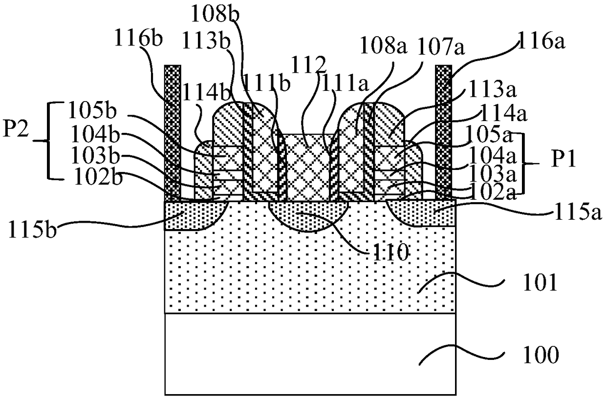
[0030] Please refer to figure 1 , the present embodiment provides a method for operating a P-channel flash memory unit with a single storage bit, and the P-channel flash memory unit includes: a semiconductor substrate 100, an N well 101, a first P-type doped region 115a, a second P-type type doped region 110, the first word line gate 108a and the first storage bit P1. Wherein, the semiconductor substrate 100 is P-type doped, the N well 101 is formed in the semiconductor substrate 100, and the first P-type doped region 115a and the second P-type doped region 110 are both formed in the semiconductor substrate 1...
PUM
 Abstract
Description
Claims
Application Information
 - R&D Engineer
- R&D Manager
- IP Professional
- Industry Leading Data Capabilities
- Powerful AI technology
- Patent DNA Extraction
Browse by: Latest US Patents, China's latest patents, Technical Efficacy Thesaurus, Application Domain, Technology Topic.
© 2024 PatSnap. All rights reserved.Legal|Privacy policy|Modern Slavery Act Transparency Statement|Sitemap