Method for fixing electronic component on PCB and finishing welding

A technology for PCB circuit boards and electronic components, which is applied in the direction of assembling printed circuits, electrical components, and printed circuits with electrical components, which can solve the problems of low production efficiency, difficult to guarantee product qualification rate, and high labor costs.

Pending Publication Date: 2018-11-13
付云
View PDF0 Cites 2 Cited by
  • Summary
  • Abstract
  • Description
  • Claims
  • Application Information

AI Technical Summary

Problems solved by technology

[0002] At present, the large-scale mass-produced circuit boards basically use the placement machine to glue the electronic components to the tin contacts at the designated positions, and then heat the solder paste to reach the melting point and then bond with the electronic components. The feet are welded as one, and then the temperature is lowered to solidify the solder paste to complete the welding of the electronic components and the PCB circuit board. However, the pressure caused by the difference in the amount of solder on the contacts of the PCB circuit board will cause some electronic components to break (damage) ), the welding quality cannot be seen intuitively, for example: there are bubbles in the solder paste, unmelted, offset contacts of the feet of electronic components, etc.; in addition, not all electronic components can be soldered by placement machines, some vertical Or larger electronic components need to be manually welded, the labor cost is high, the production efficiency is low, and manual welding of electronic components that require some positive and negative electrodes will cause reverse welding of the positive and negative electrodes, and the product qualification rate is difficult to guarantee; The cost of SMT electronic components dedicated to SMT is high

Method used


Image

  • Method for fixing electronic component on PCB and finishing welding
  • Method for fixing electronic component on PCB and finishing welding
  • Method for fixing electronic component on PCB and finishing welding

Examples


Embodiment 1

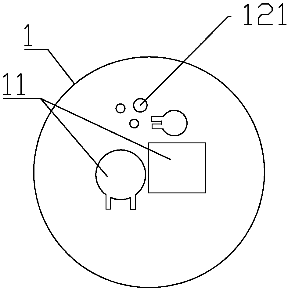
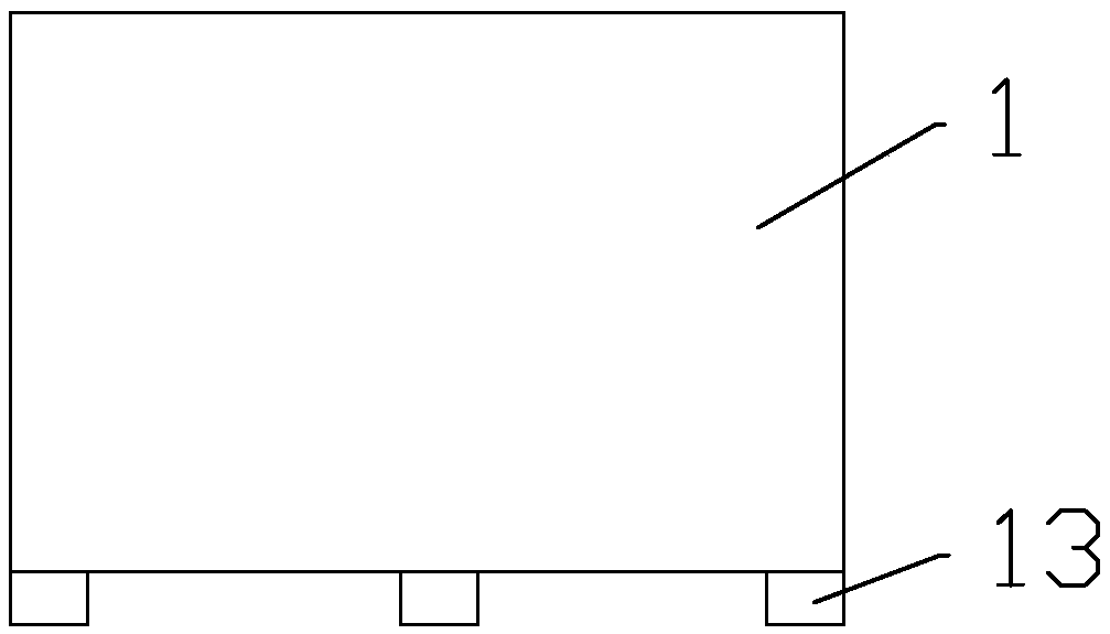
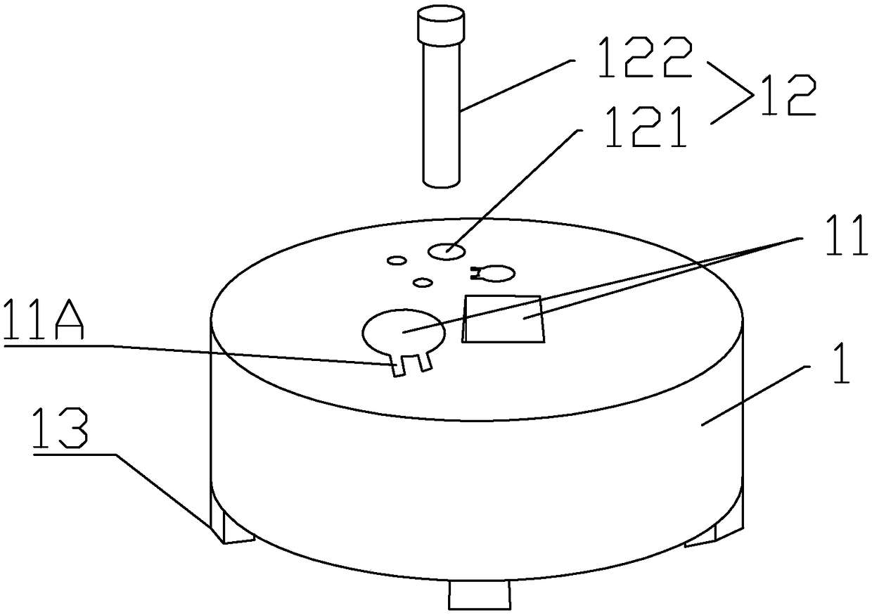
[0062] like Figure 4 , Figure 5 Shown: a method for fixing electronic components on a PCB circuit board and completing welding, including an electronic component positioning block 1 and a PCB circuit board 2, the top of the electronic component positioning block 1 is provided with a matching wire A for welding The electronic components of the designated solder paste contact A1 on the PCB circuit board 2 are inserted into the through hole 11; the positioning block 1 of the electronic components is provided with a positioning device 12 that cooperates with the PCB circuit board 2 to fix the position, and the positioning device 12 includes a positioning device located at The positioning through hole 121 on the top of the electronic component, the positioning through hole 121 is inserted with a positioning pin 122; the PCB circuit board 2 is provided with a positioning hole 21; the bottom of the positioning block 1 of the electronic component is fixed with a foot pad 13; the we...

Embodiment 2

[0071] like Image 6 , Figure 7 Shown: a method for fixing electronic components on a PCB circuit board and completing welding, including an electronic component positioning block 1 and a PCB circuit board 2, the top of the electronic component positioning block 1 is provided with a matching electronic transformer B The electronic components soldered to the specified solder paste contacts B1, B2, B3, B4 of the PCB circuit board 2 are inserted into the through holes 11; the positioning block 1 of the electronic components is provided with a positioning device 12 that cooperates with the PCB circuit board 2 to fix the position , the positioning device 12 is a positioning column; the PCB circuit board 2 is provided with a positioning aperture 21; the bottom of the electronic component positioning block 1 is fixed with a foot pad 13; the welding method includes the following steps: A, positioning: Place the electronic component positioning block 1 on the front of the PCB circuit...

Embodiment 3

[0079] like Figure 8 , Figure 9 Shown: a method for fixing electronic components on a PCB circuit board and completing welding, including an electronic component positioning block 1 and a PCB circuit board 2, and the top of the electronic component positioning block 1 is provided with a matching "L" The capacitor C of the shaped pin is welded on the PCB circuit board 2 and the electronic components of the designated solder paste contacts C1 and C2 are inserted into the through hole 11, and the wall body of the electronic component inserted into the through hole 11 is provided with a pin positioning through groove for inserting the pin of the electronic component 11A; the electronic component positioning block 1 is provided with a positioning device 12 that cooperates with the PCB circuit board 2 to fix the position, and the positioning device 12 is a positioning hole; the PCB circuit board 2 is provided with a raised rod 22; the electronic The bottom of the component positi...


PUM


Abstract

The invention discloses a method for fixing an electronic component on a PCB and finishing welding. An electronic component positioning block 1 and a PCB 2 are included, and at least one electronic component insertion through hole 11 matched with the electronic component to be welded at a designated solder paste contact of the PCB is formed in the top of the electronic component positioning block1. The welding method comprises the steps as follows: positioning, insertion of the electronic component, putting in a furnace, cooling and forming. The method has the advantages that the electronic component can be completely prevented from being broken (damaged), the welding quality is greatly improved, the reject ratio is almost zero, the production efficiency is obviously improved, pins of thewelded electronic component and solder paste are firmly connected, the pins of the welded electronic component are welded in the center, and the production cost is greatly reduced and the like.

Description

technical field [0001] The invention relates to a process for welding electronic components to a PCB circuit board, in particular to a method for fixing electronic components on a PCB circuit board and completing welding. Background technique [0002] At present, the large-scale mass-produced circuit boards basically use the placement machine to glue the electronic components to the tin contacts at the designated positions, and then heat the solder paste to reach the melting point and then bond with the electronic components. The feet are welded together, and then the temperature is lowered to solidify the solder paste to complete the welding of the electronic components and the PCB circuit board. However, the pressure caused by the difference in the amount of solder on the contacts of the PCB circuit board will cause some electronic components to break (damage) ), the welding quality cannot be seen intuitively, for example: there are bubbles in the solder paste, unmelted, o...

Claims


Application Information

Patent Timeline
Patent Type & Authority Applications(China)
IPC IPC(8): H05K3/34
CPCH05K3/3431H05K3/34
Inventor 付云
Owner 付云
Why Eureka
Try Eureka