

Manufacturing method of OLED display module group and the OLED display module group
A technology for display modules and manufacturing methods, applied in semiconductor/solid-state device manufacturing, electrical components, electric solid-state devices, etc., can solve the problems of reducing production efficiency and increasing the production process of OLED display modules, so as to improve production efficiency and improve The effect of protection, good sealing effect
Active Publication Date: 2018-11-16
TRULY SEMICON
View PDF5 Cites 0 Cited by
- Summary
- Abstract
- Description
- Claims
- Application Information
AI Technical Summary
Problems solved by technology
In this way, the production process of the OLED display module is increased, and the production efficiency is greatly reduced.
Method used
View moreImage
Smart ImageViewing Examples

Examples
Embodiment 2
[0035] This embodiment provides an OLED display module, which is obtained by using the manufacturing method of the OLED display module described in the above embodiments.
Login to View More PUM
 Abstract
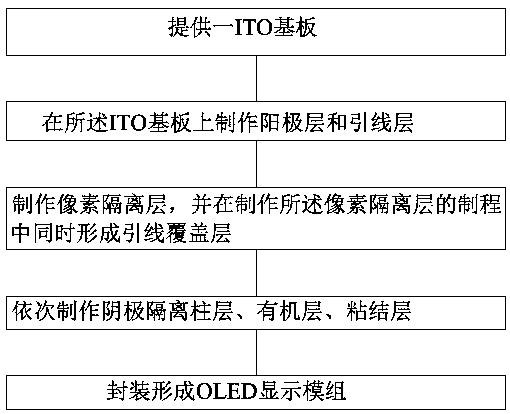
The invention provides the manufacturing method of an OLED display module group and the OLED display module group. The method comprises the following steps of step1, providing an ITO substrate; step2,manufacturing an anode layer and a lead wire layer on the ITO substrate; step3, manufacturing a pixel isolation layer, and forming a lead wire covering layer outside a packaging area in the process of manufacturing the pixel isolation layer; step4, successively manufacturing a cathode isolation pillar layer, an organic layer, a cathode layer and a bonding layer; and step5, packaging and forming the OLED display module group. By using the manufacturing method of the OLED display module group and the OLED display module group, the lead wire covering layer is formed in the process of manufacturing the pixel isolation layer so that the operation of setting the lead wire covering layer does not need to be increased and production efficiency can be effectively improved. Simultaneously, a lead wire can be timely protected and the lead wire is ensured not to be damaged or corroded.
Description
technical field [0001] The invention relates to the field of display technology, in particular to a method for manufacturing an OLED display module and the OLED display module. Background technique [0002] OLED display modules generally include a substrate, an anode layer, a lead layer, a pixel isolation layer, a cathode isolation column layer, an organic layer, a cathode layer, and an adhesive layer for packaging. The lead layer is not exposed to the air. The existing OLED display module needs to form a lead cover layer to protect the lead layer outside the package area after the package is completed, and often the adhesive layer overlaps with the cover layer. to ensure protection. In this way, the production process of the OLED display module is increased, and the production efficiency is greatly reduced. Contents of the invention [0003] The technical problem to be solved by the invention is to effectively form the lead covering layer and improve the production effi...
Claims
Login to View More Application Information
Patent Timeline
 Patent Type & AuthorityApplications(China)
IPC IPC(8): H01L51/56H01L51/52H01L27/32
CPCH10K59/12H10K50/844H10K71/00
Inventor田宁陈芳刘然赵云
OwnerTRULY SEMICON