Common voltage generation circuit, source drive circuit and liquid crystal display device
A common voltage and generating circuit technology, which is applied in the field of source drive circuits, liquid crystal display devices, and common voltage generating circuits, can solve problems such as reverse color of liquid crystal display panels, and achieve the effect of avoiding reverse color phenomenon
- Summary
- Abstract
- Description
- Claims
- Application Information
AI Technical Summary
Problems solved by technology
Method used
Image
Examples
no. 1 example
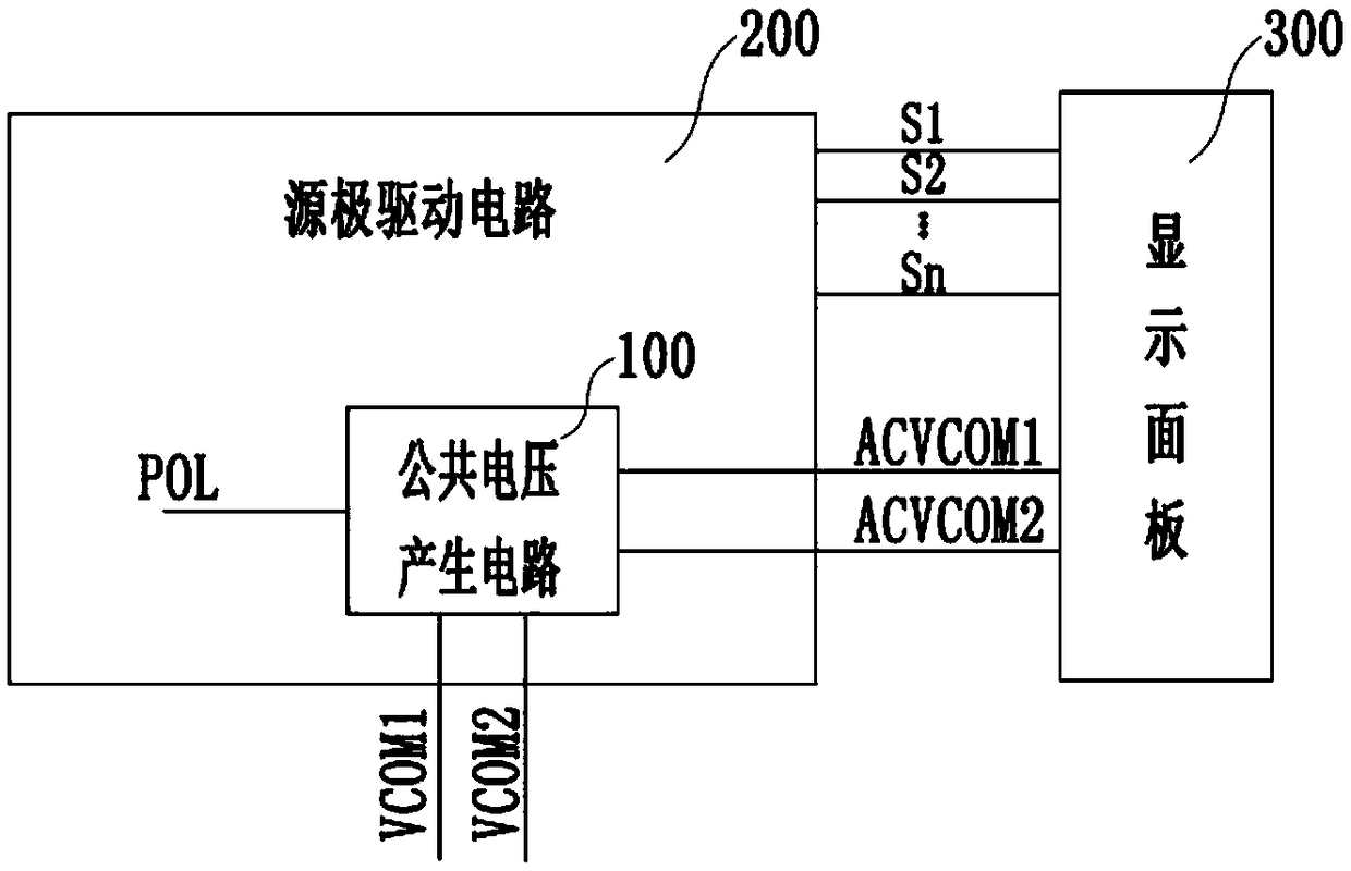
[0025] Please refer to figure 1 , figure 1 It is a schematic connection diagram of a common voltage generating circuit of an embodiment. Such as figure 1 As shown, the common voltage generating circuit of this embodiment includes a common voltage generating circuit 100, the common voltage generating circuit 100 receives the first common voltage VCOM1 and the second common voltage VCOM2, and reverses the polarity according to the output of the source driving circuit 200 The control signal POL outputs the first AC common voltage ACVCOM1 and the second AC common voltage ACVCOM2 with opposite polarities, and the first AC common voltage ACVCOM1 or the second AC common voltage ACVCOM2 and the source driving circuit 200 output on the corresponding data line data signal ( figure 1 S1, S2 . . . Sn) have the same polarity, and the data signal and the AC common voltage with the same polarity as the data signal act together on the same pixel unit of the display panel 300 .
[0026] Sp...
no. 2 example
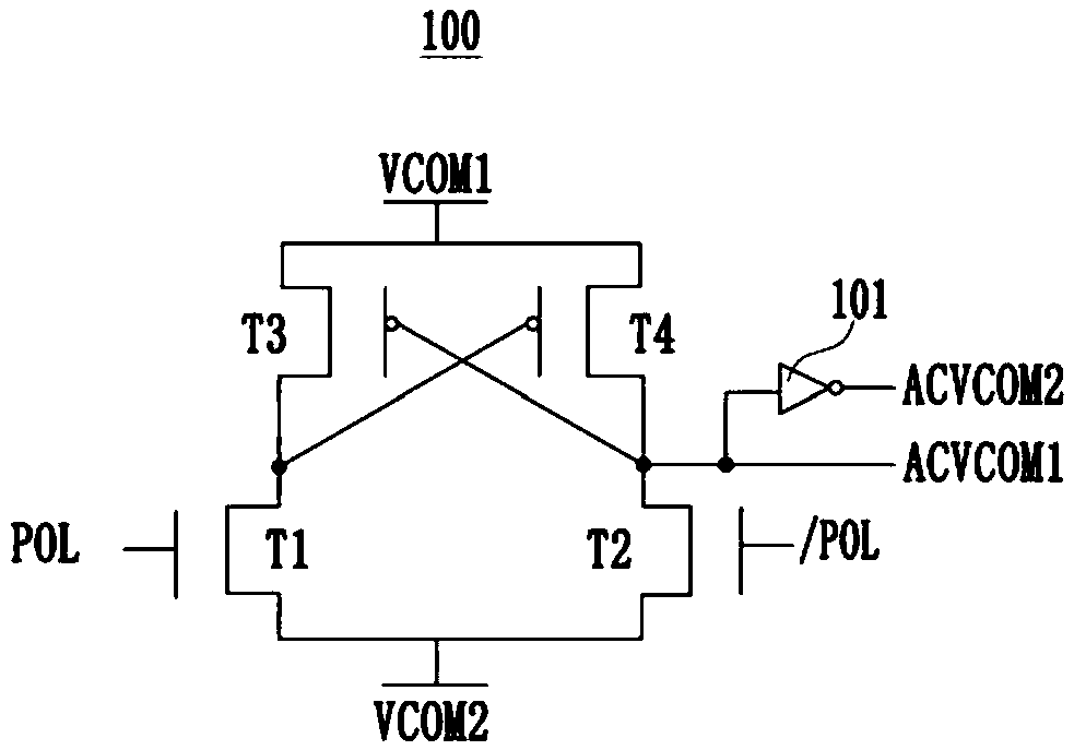
[0032] figure 2 It is a circuit connection diagram of a common voltage generating circuit of an embodiment. Such as figure 2 As shown, this embodiment provides a specific circuit connection of the common voltage generating circuit 100 in the common voltage generating circuit. The common voltage generating circuit 100 includes a first switching element T1 , a second switching element T2 , a third switching element T3 , a fourth switching element T4 and a first inverting element 101 . The first switch element T1 includes a first control terminal, a first channel terminal and a second channel terminal, the first control terminal of the first switch element T1 receives the polarity inversion control signal POL, and the second channel terminal of the first switch element T1 Receive the second common voltage VCOM2. The second switch element T2 includes a second control terminal, a third channel terminal, and a fourth channel terminal. The second control terminal of the second s...
no. 3 example
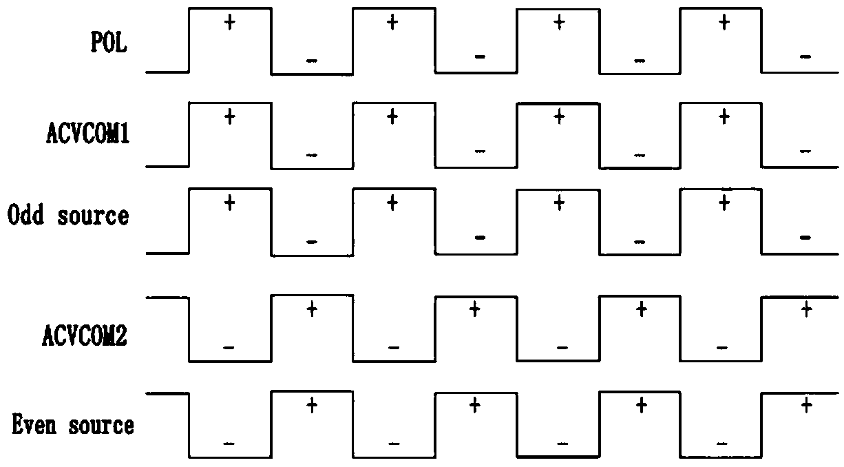
[0042] image 3 It is a related waveform diagram of the output voltage of the common voltage generating circuit of an embodiment. In this example, the polarity of the first AC common voltage ACVCOM1 is the same as that of the data signal output by the source driver circuit 200 on the data lines of odd columns, and the second AC common voltage ACVCOM2 is consistent with the polarity of the data signals output by the source driver circuit 200 on the data lines of even columns. The polarity of the output data signal on the same, and can be obtained as image 3 The waveform diagram shown.
[0043] Specifically, the polarities of the first AC common voltage ACVCOM1 and the second AC common voltage ACVCOM2 follow each polarity reversal of the polarity reversal control signal POL, and, through the first AC common voltage ACVCOM1 and the source The polarity of the data signal Odd Source output by the electrode drive circuit 200 on the data lines of odd columns is consistent, so that...
PUM
 Abstract
Description
Claims
Application Information


