
Light-emitting element, light-emitting element array and light-emitting device thereof

A technology of light-emitting elements and light-emitting devices, which is applied in the direction of electrical components, electric solid-state devices, semiconductor devices, etc., can solve problems such as pulling at the edge of the chip, large internal stress of gallium nitride, collapse and fragmentation, etc., to reduce residues and shorten the manufacturing process Time, the effect of reducing the probability of collapse

Active Publication Date: 2018-11-23
XIAMEN SANAN OPTOELECTRONICS CO LTD
View PDF5 Cites 0 Cited by
  • Summary
  • Abstract
  • Description
  • Claims
  • Application Information

AI Technical Summary

Problems solved by technology

[0002] Conventional thin-film LED chip structure, when using laser to peel off the sapphire substrate, there are following problems, such as: when the sapphire substrate is peeled off, there will be a pulling phenomenon at the edge of the chip, so that the epitaxial layer is pulled and broken, and the cracks may extend to When the sapphire substrate is peeled off, due to the extremely high internal stress of GaN, part of the epitaxial layer at the edge has no support structure, which causes collapse and fragmentation, and the cracks may extend into the chip structure and cause destroy

Method used


Image

  • Light-emitting element, light-emitting element array and light-emitting device thereof
  • Light-emitting element, light-emitting element array and light-emitting device thereof
  • Light-emitting element, light-emitting element array and light-emitting device thereof

Examples


Embodiment Construction

[0061]The implementation of the present invention will be described in detail below in conjunction with the accompanying drawings and examples, so as to fully understand and implement the process of how to apply technical means to solve technical problems and achieve technical effects in the present invention. It should be noted that, as long as there is no conflict, each embodiment and each feature in each embodiment of the present invention can be combined with each other, and the formed technical solutions are all within the protection scope of the present invention.

[0062] It should be understood that the terminology used in the present invention is only for the purpose of describing specific embodiments, rather than limiting the present invention. It is further understood that when the terms "comprising" and "comprising" are used in the present invention, they are used to indicate the existence of stated features, integers, steps, elements, and / or, without excluding one ...


PUM


Abstract

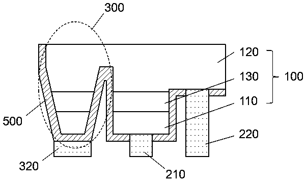
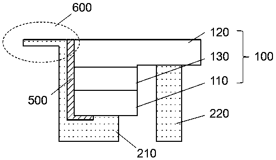
The invention provides a light-emitting device, having a substrate including a control circuit, wherein the light-emitting device includes a light-emitting element, and the light-emitting element hasa semiconductor layer sequence that includes a first type semiconductor layer, a second type semiconductor layer and an active light-emitting layer between the first type semiconductor layer and the second type semiconductor layer; the light-emitting device has a sacrificial structure, the light-emitting element is connected to the control circuit of the substrate, the light-emitting element has adopted or will adopt a process of laser stripping substrate, and the sacrificial structure prevents the light-emitting element from being damaged caused by too large peeling impact force when the substrate is being peeled off.

Description

technical field [0001] The invention belongs to the field of semiconductor manufacturing, and in particular relates to a light emitting element, an array of light emitting elements and a light emitting device thereof. Background technique [0002] Conventional thin-film LED chip structure, when using laser to peel off the sapphire substrate, there are following problems, such as: when the sapphire substrate is peeled off, there will be a pulling phenomenon at the edge of the chip, so that the epitaxial layer is pulled and broken, and the cracks may extend to When the sapphire substrate is peeled off, due to the extremely high internal stress of GaN, part of the epitaxial layer at the edge has no support structure, which causes collapse and fragmentation, and the cracks may extend into the chip structure and cause destroy. Contents of the invention [0003] The present invention proposes a feasible solution to the problems in the background technology, through which a high...

Claims


Application Information

Patent Timeline
IPC IPC(8): H01L33/02H01L33/12H01L33/46H01L27/15
CPCH01L27/15H01L33/02H01L33/12H01L33/46
Inventor 丁绍滢范俊峰李佳恩徐宸科
Owner XIAMEN SANAN OPTOELECTRONICS CO LTD
Learn More