Optical body and light emitting device
An optical body and light-emitting area technology, applied in optics, lighting devices, optical components, etc., can solve the problem that the visual identifier cannot recognize the existence of the light guide plate, and achieve excellent functions and excellent anti-reflection effects.
- Summary
- Abstract
- Description
- Claims
- Application Information
AI Technical Summary
Problems solved by technology
Method used
Image
Examples
Embodiment 1
[0116] (1-1. Fabrication of Optical Body)
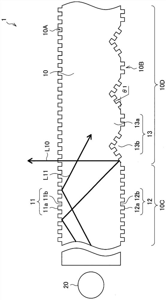
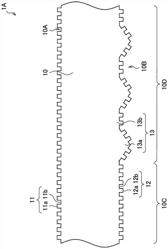
[0117] Figure 7 It shows the structure of the optical body 1-1 which concerns on Example 1. In Example 1, the optical body 1-1 was produced through the following process. First, as a substrate 10-1, a polymethyl methacrylate film (manufactured by Sumika Acrylic Sales Co., Ltd., Technolloy) having a thickness of 150 μm was prepared. Next, use Image 6 The transfer apparatus 300 shown in 10 forms the second fine concave-convex structure 12 on one surface (here, the second surface 10B) of the substrate 10-1. Here, as the photocurable resin composition, an ultraviolet curable acrylic resin composition (SK1120 manufactured by Dexerials Corporation) was used. In addition, in order to improve the adhesiveness of the substrate 10-1 and the cured layer of the uncured resin layer, the second surface 10B of the substrate 10-1 is subjected to primer treatment in advance. By the primer treatment, a primer layer having a thickness of approxi...
Embodiment 2
[0136] (2-1. Fabrication of Optical Body)
[0137] Figure 8The structure of the optical body 1-2 concerning Example 2 is shown. In Example 2, the optical body 1-2 was produced by using the optical body 1-1 as a transfer mold. Specifically, first, the substrate 10-1 used in Example 1 was prepared. Next, primer treatment is performed on both surfaces of the base material 10-1 in order to improve the adhesiveness between the base material 10-1 and each cured layer described later. The details of the primer treatment were the same as in Example 1. A primer layer having a thickness of approximately 3 μm was formed on both surfaces of the substrate 10-1 by the primer treatment. Next, an uncured resin layer of the photocurable resin composition is formed on one surface (here, the second surface 10B) of the base material 10-1. Next, the shape of the second surface 10B of the optical body 1 - 1 , that is, the second fine uneven structure 12 and the coarse uneven structure 13 is t...
Embodiment 3
[0142] (3-1. Fabrication of Optical Body)
[0143] Figure 9 It shows the structure of the optical body 1-3 which concerns on Example 3. Optical body 1-2 was used as a transfer mold in Example 3 to produce optical body 1-3. Specifically, first, the substrate 10-1 used in Example 1 was prepared. Next, primer treatment is performed on both surfaces of the base material 10-1 in order to improve the adhesiveness between the base material 10-1 and each cured layer described later. The details of the primer treatment were the same as in Example 1. A primer layer having a thickness of approximately 3 μm was formed on both surfaces of the substrate 10-1 by the primer treatment. Next, an uncured resin layer of the photocurable resin composition is formed on one surface (here, the second surface 10B) of the substrate 10-1. Next, the shape of the second surface 10B of the optical body 1-2, that is, the second fine uneven structure 12 and the coarse uneven structure 13 is transferred...
PUM
| Property | Measurement | Unit |
|---|---|---|
| height | aaaaa | aaaaa |
| height | aaaaa | aaaaa |
| thickness | aaaaa | aaaaa |
Abstract
Description
Claims
Application Information


