Wafer marking monitoring method and laser marking machine alignment position determination method
A marking and wafer technology, applied in semiconductor/solid-state device testing/measurement, electrical components, circuits, etc., can solve problems such as whether the optical path orientation is abnormal, difficult, and the shape of the wafer mark cannot be determined
- Summary
- Abstract
- Description
- Claims
- Application Information
AI Technical Summary
Problems solved by technology
Method used
Image
Examples
Embodiment Construction
[0027] The present invention is described in detail below in conjunction with accompanying drawing:
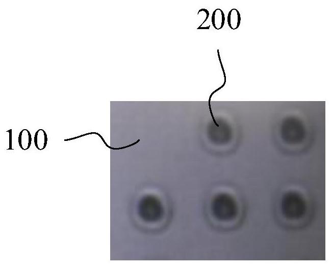
[0028] Please refer to figure 1 , a plurality of wafer marks 200 are formed on the wafer 100 .
[0029] Embodiments of the present invention provide a method for monitoring wafer markings, comprising the following steps:
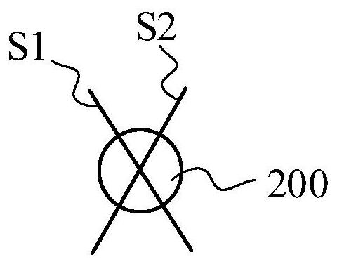
[0030] Step 1, please refer to Figure 3 to Figure 7 , in the horizontal plane of the wafer mark 200, scan the wafer mark 200 in two intersecting directions to obtain two sets of waveform signals in corresponding directions, which are respectively denoted as the first waveform signal Q1 and the second waveform signal Q2; wherein, the two intersecting directions Including the first direction S1 and the second direction S2.
[0031] Step 2, please refer to Figure 8 to Figure 9 , measure the diameter length of the same wafer mark 200 in two sets of waveform signals; that is, measure the first diameter length D1 of the first waveform signal Q1 obtained by s...
PUM
 Abstract
Description
Claims
Application Information


