Notch defect detection method for flexible IC package substrate line

A packaging substrate and defect detection technology, which is applied in the field of image processing, can solve the problems of sub-pixel accuracy, inability to detect the position of the curve, and complicated methods.

Active Publication Date: 2018-11-30
SOUTH CHINA UNIV OF TECH
View PDF8 Cites 16 Cited by
  • Summary
  • Abstract
  • Description
  • Claims
  • Application Information

AI Technical Summary

Problems solved by technology

However, Hough transform can only detect straight lines, but cannot detect the position of curves, and it is a transformation method based on pixel calculation, which does not achieve sub-pixel accuracy, so it is difficult to accurately locate the position of straight lines.
When the Radon transform is used, sub-pixel accuracy can be achieved, but the general Radon transform cannot locate the starting point of the straight line, so the detected straight line spans the entire image, and the length of the straight line cannot be accurately measured.
For the detection of curves, there are generally g

Method used


Image

  • Notch defect detection method for flexible IC package substrate line
  • Notch defect detection method for flexible IC package substrate line
  • Notch defect detection method for flexible IC package substrate line

Examples


Embodiment

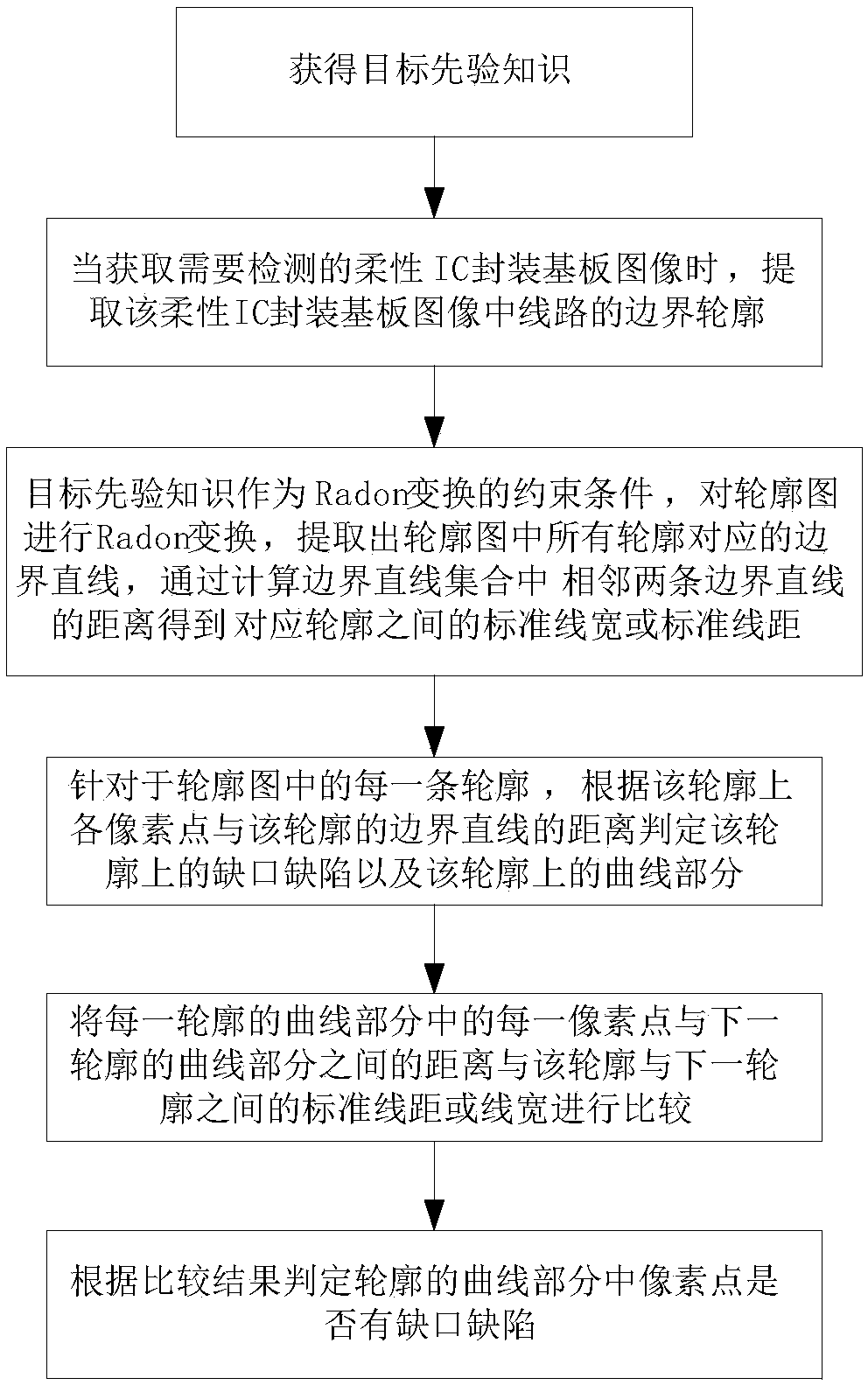
[0071] This embodiment discloses a method for detecting notch defects of flexible IC packaging substrate circuits, such as figure 1 As shown, the steps are as follows:

[0072] Step S1, select a flexible IC packaging substrate of the same type as the flexible IC packaging substrate that needs to detect notch defects, and randomly select some images of the above-mentioned flexible IC packaging substrate, and then pre-learn the circuit features therein to obtain target prior knowledge;

[0073] Wherein in this embodiment, this step pre-learns the circuit features in the flexible IC packaging substrate image, and the specific process of obtaining the target prior knowledge is as follows:

[0074] Statistics the data of the points in the Radon graph corresponding to the two parallel boundary lines in the selected flexible IC package substrate image, and select the maximum inclination angle difference ε° corresponding to the two parallel boundary lines and the value of the center p...


PUM


Abstract

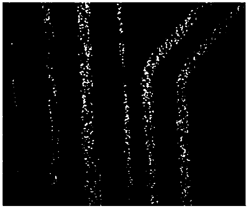
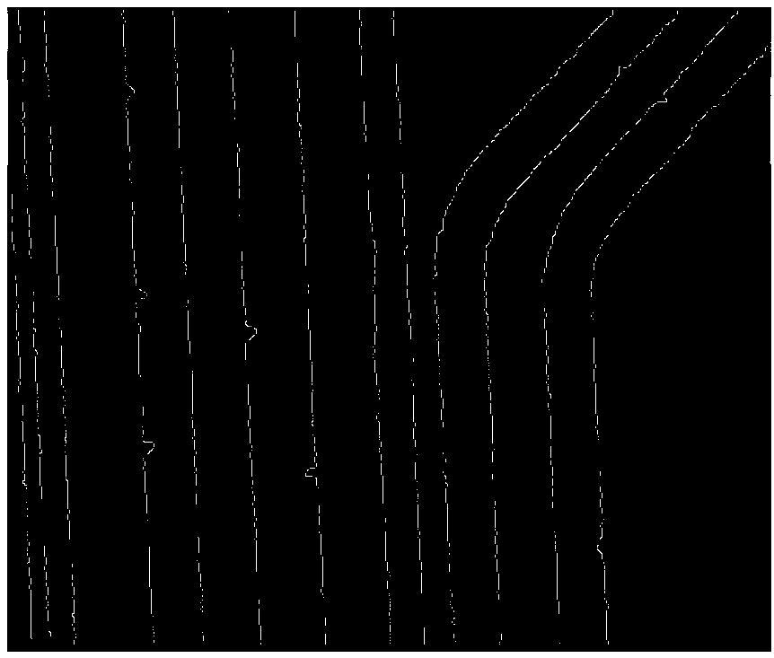
The invention discloses a notch defect detection method for a flexible IC package substrate line. The method comprises the following steps: obtaining target prior knowledge; extracting a boundary contour of a line of a flexible IC package substrate image to be detected to obtain a contour map; using the target prior knowledge as the constraint condition of Radon transform to carry out Radon transform on the contour map, extracting the boundary line in the contour map, and calculating a standard line width or a standard line space between the contours through the boundary line; determining a notch defect on the contour and a curve portion on the contour by aiming at each contour in the contour map; comparing the distance between each pixel point in the curve portion of each contour and thecurved portion of the next contour with the standard line space or the line width between the contour and the next contour, and determining whether the pixel point in the curve portion of the contourhas the notch defect or not according to the comparison result. The method can accurately and quickly detect the notch defects of the linear portion and the curve portion.

Description

technical field [0001] The invention relates to the technical field of image processing, in particular to a method for detecting notch defects of flexible IC packaging substrate circuits. Background technique [0002] The automatic detection technology of the circuit size of the high-density flexible IC packaging substrate can realize the detection of the circuit size of the micron-level high-density flexible IC packaging substrate, thereby improving the detection efficiency of the production line. The image straight line and curve detection involved is a very important field of numerical image processing. Dimensional inspection of high-density flexible IC packaging substrate circuits requires precise positioning of the straight and curved parts of the circuit contour, and different calculation methods are required for the straight and curved parts to mark the notch defects of the circuit contour. Therefore, a new method for detecting and locating notch defects is of great ...

Claims


Application Information

Patent Timeline
IPC IPC(8): G01N21/88
CPCG01N21/8851G01N2021/8887
Inventor 罗家祥邹恒胡跃明
Owner SOUTH CHINA UNIV OF TECH
Why Eureka
Try Eureka