Pixel driving circuit and display panel

A pixel drive circuit and drive signal technology, applied in static indicators, instruments, etc., can solve the problems of uneven light emission of light-emitting devices OLED, affecting image quality, attenuation of light-emitting materials, etc., to avoid afterimage phenomenon, uniform and stable light emission , The effect of eliminating the influence of the threshold voltage on the drive current

Inactive Publication Date: 2018-12-07
WUHAN CHINA STAR OPTOELECTRONICS SEMICON DISPLAY TECH CO LTD
View PDF5 Cites 2 Cited by
  • Summary
  • Abstract
  • Description
  • Claims
  • Application Information

AI Technical Summary

Problems solved by technology

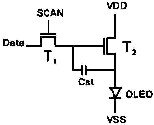
[0003] The current I when the light-emitting device OLED emits light OLED is the current corresponding to the gate-source voltage Vgs of the drive transistor T2, the current I OLED can be expressed by the following equation, I OLED =k(Vgs-Vth)2=k(VDD-VData-|Vth|)2, as can be seen from the equation, in the above-mentioned pixel drive circuit, the current I OLED Depends on the threshold voltage Vth of the driving transistor T2, so the variation of the threshold voltage in the driving transistor T2 will cause the light-emitting device OLED to emit unevenly and affect the image quality
[0004] In addition, due to the principle of self-luminescence, the attenuation of the luminescent material occurs after the same pixel maintains the same brightness for a long time

Method used


Image

  • Pixel driving circuit and display panel
  • Pixel driving circuit and display panel
  • Pixel driving circuit and display panel

Examples


Embodiment Construction

[0039] The liquid crystal display assembly provided by the embodiment of the present invention has been introduced in detail above. The principles and implementation modes of the present invention are explained by using specific examples in this paper. The description of the above embodiments is only for helping to understand the present invention. At the same time, for those skilled in the art, according to the idea of ​​the present invention, there will be changes in the specific implementation and application scope. In summary, the content of this specification should not be construed as limiting the present invention. The following descriptions of the various embodiments refer to the accompanying drawings to illustrate specific embodiments in which the invention may be practiced. The directional terms mentioned in the present invention, such as [top], [bottom], [front], [back], [left], [right], [inside], [outside], [side], etc., are only for reference The orientation of th...


PUM


Abstract

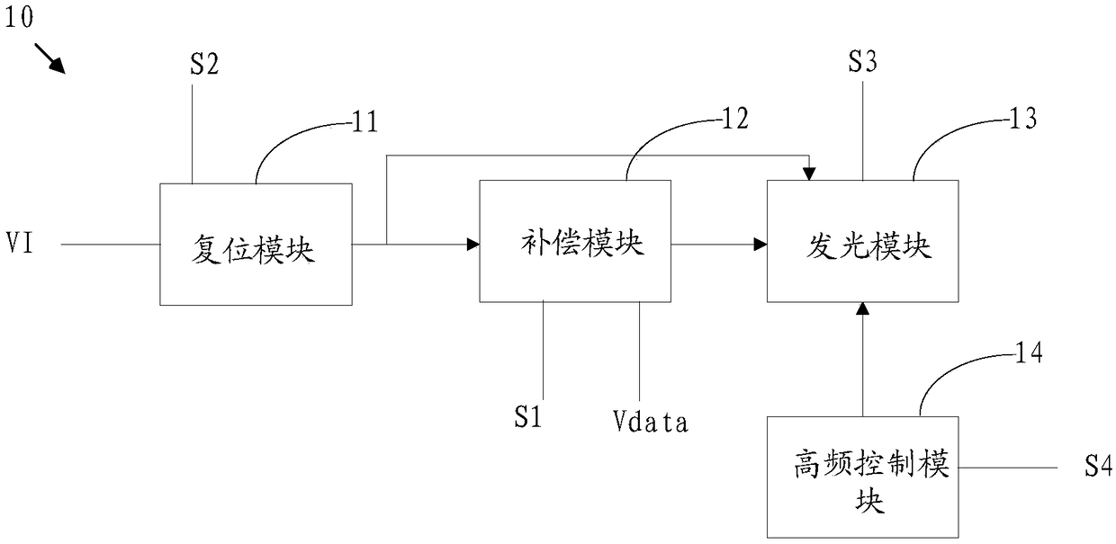
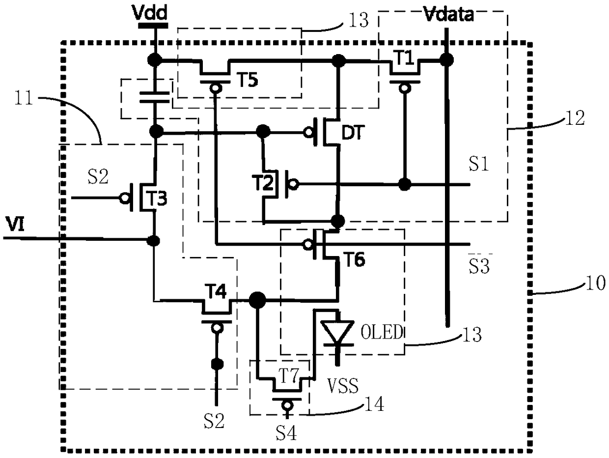
The invention provides a pixel driving circuit and a display panel. A high-frequency control module is additionally arranged, the high-frequency control module controls the light emitting efficiency of a light emitting device under control of a high-frequency control signal, and a light emitting material is avoided from a mura phenomenon due to attenuation caused by that current passes the material for a long time; and in addition, influence of a threshold voltage of a driving transistor on the driving current can be eliminated, so that the light emitting device can emit light more uniformly and stably.

Description

technical field [0001] The present invention relates to the field of display technology, in particular to a pixel driving circuit and a display panel. Background technique [0002] see figure 1 , figure 1 It is a structural schematic diagram of an existing pixel driving circuit. Such as figure 1 As shown, the existing pixel driving circuit includes a light emitting device OLED, a driving transistor T2, a switching transistor T1 and a storage capacitor Cst. Wherein, the storage capacitor Cst stores the threshold voltage of the driving transistor T2, one end of the storage capacitor Cst is connected to the control end of the driving transistor T2 and the second end of the switching transistor T1, and the other end of the storage capacitor Cst is connected to the second end of the driving transistor T2 and the second end of the switching transistor T1. The anode of the light emitting device OLED is connected; the control terminal of the switching transistor T1 is connected ...

Claims


Application Information

Patent Timeline
Patent Type & Authority Applications(China)
IPC IPC(8): G09G3/3233
Inventor 谢锐
Owner WUHAN CHINA STAR OPTOELECTRONICS SEMICON DISPLAY TECH CO LTD
Why Eureka
Try Eureka