
A kind of preparation method of zinc oxide thin film transistor
A zinc oxide thin film and transistor technology, applied in the direction of transistors, semiconductor/solid-state device manufacturing, semiconductor devices, etc., can solve the problems of poor electrical stability, low on-state current, etc., achieve high on-state current, low cost, and simple preparation process Effect
- Summary
- Abstract
- Description
- Claims
- Application Information
AI Technical Summary
Problems solved by technology
Method used
Image

Examples
Embodiment Construction
[0079] Include the following steps:
[0080] (1), clean the substrate 1, the substrate 1 adopts a hard substrate or a flexible substrate, and the substrate of this embodiment adopts glass; the specific steps are as follows:
[0081] (1) First put the substrate 1 into an acetone solution, and ultrasonically clean it at room temperature for 3 to 5 minutes to remove surface molecular contamination;
[0082] (2) Place the substrate 1 treated in step (1) in an ethanol solution, and ultrasonically clean it at room temperature for 3 to 5 minutes to remove residual acetone on the surface;
[0083] (3) Ultrasonic cleaning the substrate 1 treated in step (2) with deionized water at room temperature for 3 to 5 minutes to remove residual ethanol and ionic contamination;
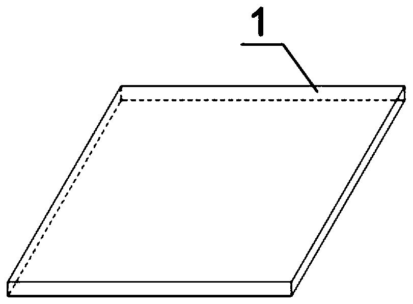
[0084] (4) Dry the substrate 1 treated in step (3) with high-purity nitrogen, and put it in an oven for 5 minutes at 90°C, see figure 1 ;
[0085] (2) Deposition of the gate 2, the gate material is a metal or oxide co...
PUM
 Abstract
Description
Claims
Application Information