Fan-out type packaging structure and manufacturing method thereof

A packaging structure and manufacturing method technology, which is applied in semiconductor/solid-state device manufacturing, electrical components, electrical solid-state devices, etc., can solve problems that affect the reliability of product packaging, the adhesive layer is easily deformed and twisted, and slippage is difficult to control, etc. , to achieve high reliability, avoid welding tolerances, and reduce process difficulty

Inactive Publication Date: 2018-12-07
NAT CENT FOR ADVANCED PACKAGING
View PDF3 Cites 12 Cited by
  • Summary
  • Abstract
  • Description
  • Claims
  • Application Information

AI Technical Summary

Problems solved by technology

However, because the adhesive layer is easily deformed and twisted, it greatly affects the reliability of product packaging and reduces product performance
In addition, the slip caused by the shrinkage of the plastic sealing material is also difficult to control

Method used


Image

  • Fan-out type packaging structure and manufacturing method thereof
  • Fan-out type packaging structure and manufacturing method thereof
  • Fan-out type packaging structure and manufacturing method thereof

Examples


Embodiment Construction

[0032] In the following description, the present invention is described with reference to various examples. One skilled in the art will recognize, however, that the various embodiments may be practiced without one or more of the specific details, or with other alternative and / or additional methods, materials, or components. In other instances, well-known structures, materials, or operations are not shown or described in detail so as not to obscure aspects of the various embodiments of the invention. Similarly, for purposes of explanation, specific quantities, materials and configurations are set forth in order to provide a thorough understanding of embodiments of the invention. However, the invention may be practiced without these specific details. Furthermore, it should be understood that the various embodiments shown in the drawings are illustrative representations and are not necessarily drawn to scale.

[0033] In this specification, reference to "one embodiment" or "the...


PUM


Abstract

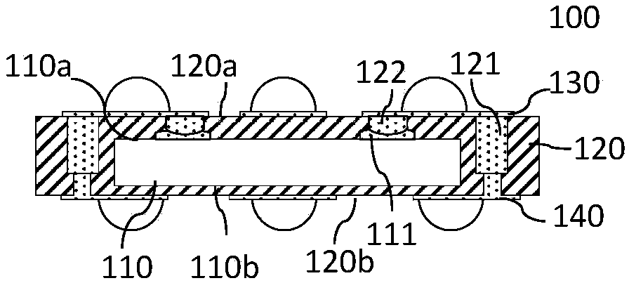
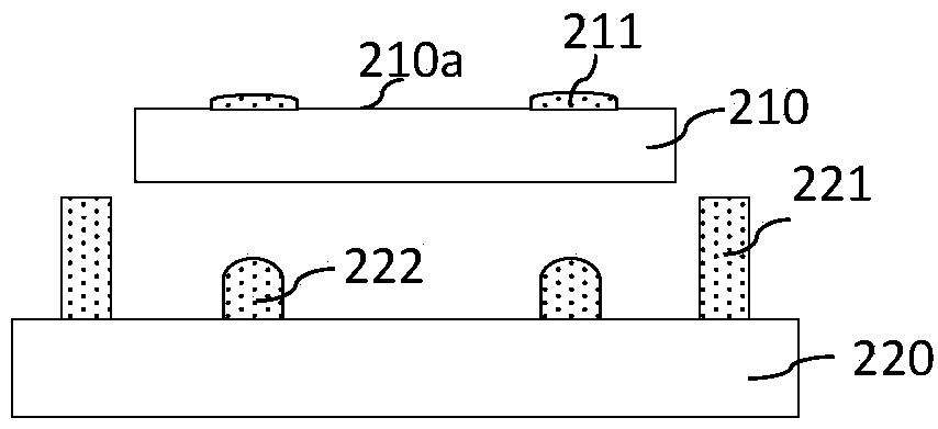
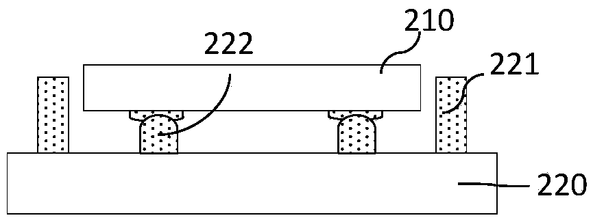
The invention discloses a fan-out type packaging structure comprising a chip and a plastic packaging layer that wraps the chip; the chip has a first surface that includes a conductive pad; the plasticpackaging layer comprises a first surface and a second surface, wherein the second surface is opposite to the first surface; the first surface is provided with a first rewiring structure, and the second surface is provided with a second rewiring structure; the plastic packaging layer also comprises a first conductive pillar that penetrates the first and second surfaces; the first conductive pillar forms an electric connection between the first rewiring structure and the second rewiring structure; the plastic packaging layer also comprises a second conductive pillar that extends from the firstsurface to the conductive pad of the chip; the electric connection is formed between the chip and the first rewiring structure.

Description

technical field [0001] The invention relates to the technical field of semiconductor packaging, in particular, the invention relates to a fan-out packaging structure and a manufacturing method thereof. Background technique [0002] In order to meet the increasingly miniaturized, intelligent, high-performance and high-reliability development of electronic products, the miniaturization and intelligence of chips have led to an increase in the number of chip package pins, and the size of package pins is also rapidly increasing. decline. In conventional flip-chip WLP schemes, the I / O connection terminals are scattered within the surface area of ​​the chip, thereby limiting the number of I / O connections. Fan-out wafer-level packaging can solve this problem very well. At the same time, due to its advantages of miniaturization, low cost and high integration, it is rapidly becoming the choice of new chip and wafer-level packaging technology. [0003] Existing fan-out packaging usua...

Claims


Application Information

Patent Timeline
Patent Type & Authority Applications(China)
IPC IPC(8): H01L21/56H01L23/00H01L23/31H01L23/522
CPCH01L21/56H01L23/3114H01L23/522H01L24/42H01L2224/04105H01L2224/12105H01L2224/96
Inventor 任玉龙孙鹏
Owner NAT CENT FOR ADVANCED PACKAGING
Why Eureka
Try Eureka