Device and method for depositing oxide film through atom layer deposition technology

A technology of oxide film and atomic layer deposition, which is applied in coating, gaseous chemical plating, metal material coating process, etc., can solve the problem of high micro pinhole defect rate and achieve the effect of reducing pinhole rate

Active Publication Date: 2018-12-11
SHANGHAI UNIV
View PDF4 Cites 2 Cited by
  • Summary
  • Abstract
  • Description
  • Claims
  • Application Information

AI Technical Summary

Problems solved by technology

[0003] The object of the present invention is to provide a device and method for depositing an oxide film using atomic layer deposition technology to solve the problem of high micro pinhole defect rate of the oxide film prepared in the prior art

Method used


Image

  • Device and method for depositing oxide film through atom layer deposition technology
  • Device and method for depositing oxide film through atom layer deposition technology
  • Device and method for depositing oxide film through atom layer deposition technology

Examples


Embodiment Construction

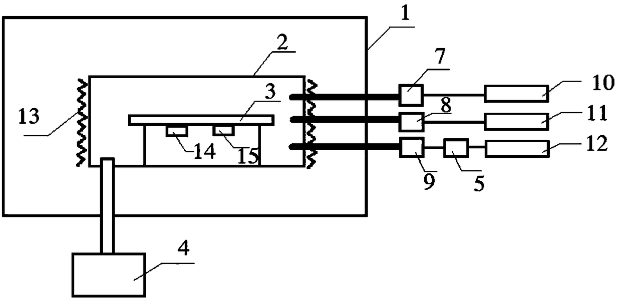
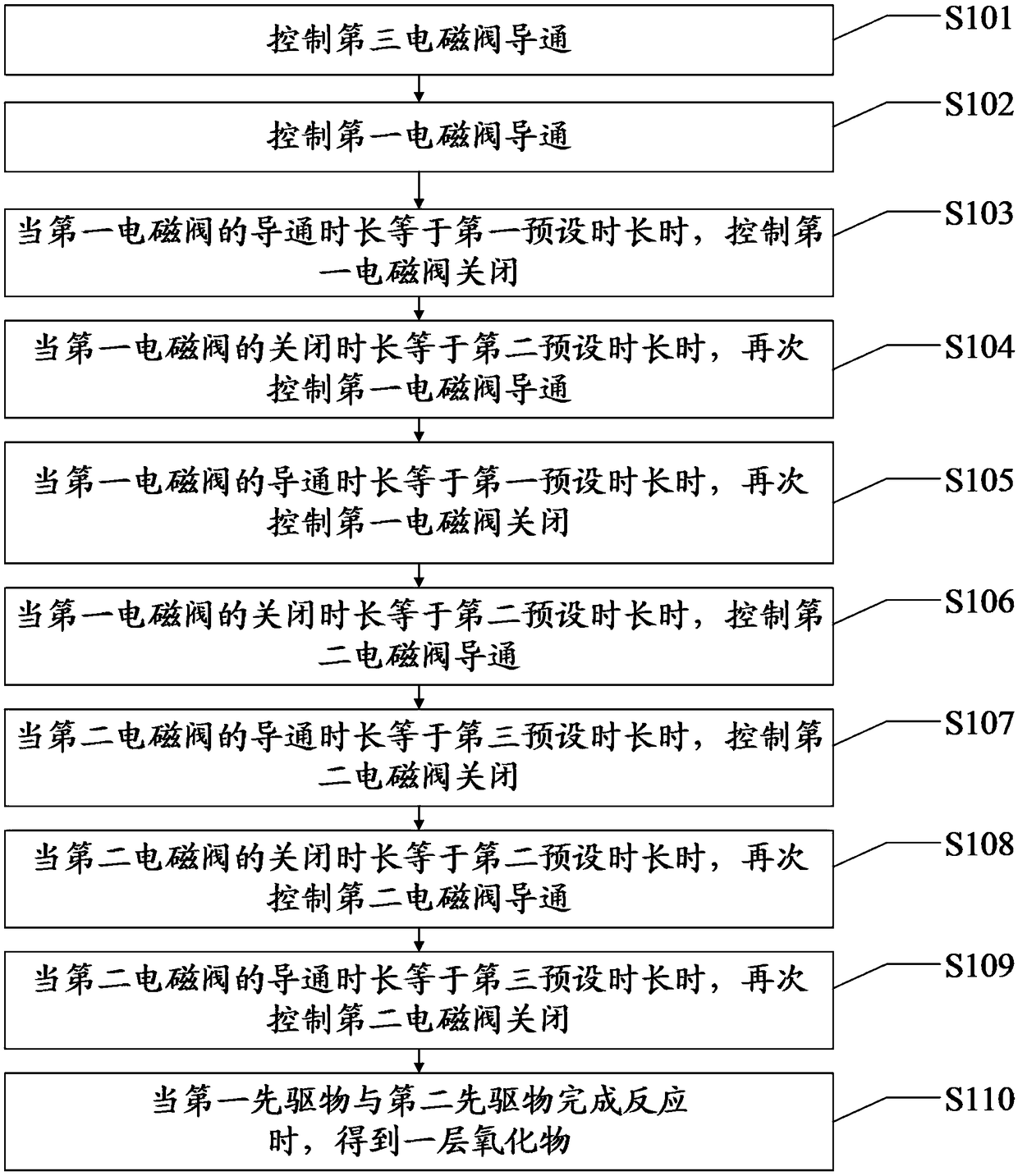
[0046] The following will clearly and completely describe the technical solutions in the embodiments of the present invention with reference to the accompanying drawings in the embodiments of the present invention. Obviously, the described embodiments are only some, not all, embodiments of the present invention. Based on the embodiments of the present invention, all other embodiments obtained by persons of ordinary skill in the art without making creative efforts belong to the protection scope of the present invention.

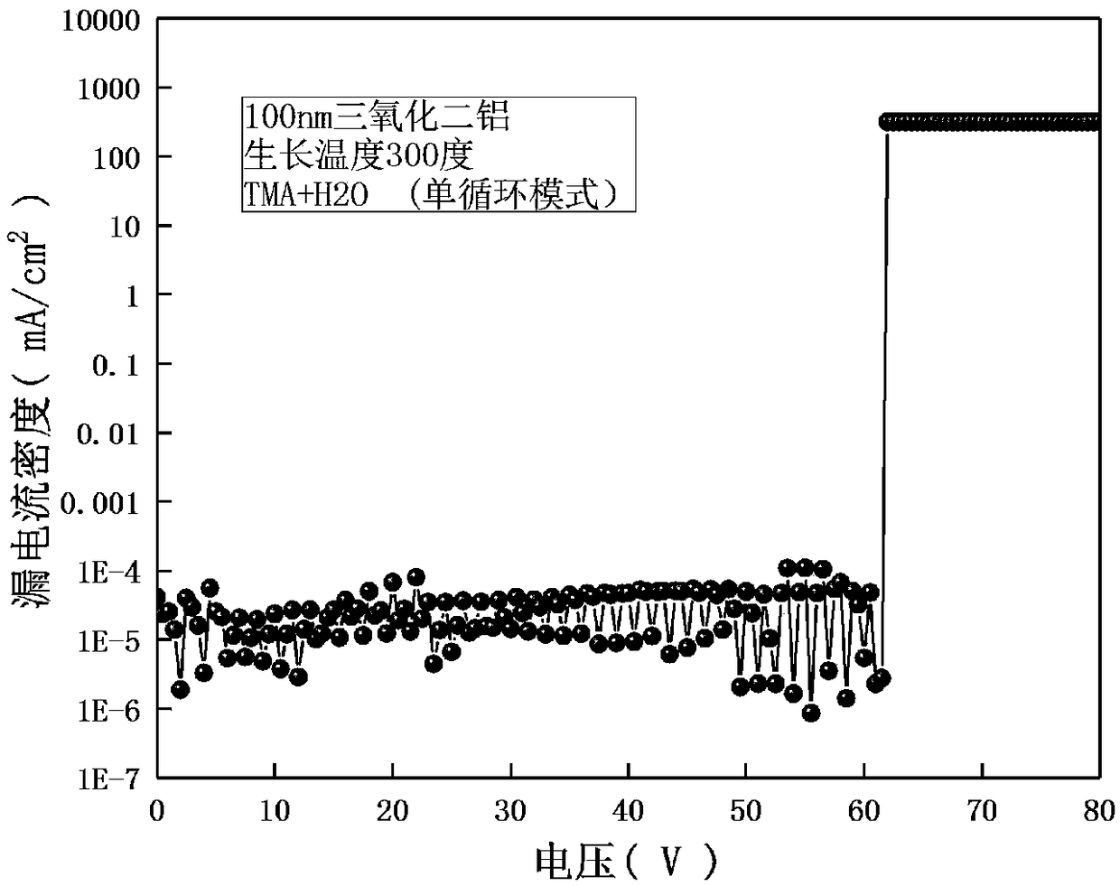
[0047] The object of the present invention is to provide a device and method for depositing an oxide film by atomic layer deposition technology, so as to solve the problem of high micro pinhole defect rate of the oxide film prepared in the prior art.

[0048] In order to make the above objects, features and advantages of the present invention more comprehensible, the present invention will be further described in detail below in conjunction with the accompanyin...


PUM


Abstract

The invention discloses a device and a method for depositing an oxide film through an atom layer deposition technology. The method comprises the following steps: controlling a third solenoid valve toconduct, and closing after controlling a first solenoid valve to conduct for first preset time length; conducting after controlling the first solenoid valve to close for second preset time length; closing after controlling the first solenoid valve to conduct for the first preset time length; conducting a second solenoid valve after controlling the first solenoid valve to close for the second preset time length; closing after controlling the second solenoid valve to conduct for third preset time length; conducting after controlling the second solenoid valve to close for the second preset time length; closing after controlling the second solenoid valve to conduct for the third preset time length, thereby completing preparation of one layer of oxides, and repeating the preparation process forone layer of the oxides by many times to obtain the oxide film. The method for depositing the oxide film is used for continuously introducing a first precursor into the device for depositing the oxide film twice, and continuously introducing a second precursor twice after adopting nitrogen gas purging, so that a pinhole rate of the deposited oxide film is reduced.

Description

technical field [0001] The invention relates to the technical field of semiconductors, in particular to a device and method for depositing an oxide film by using atomic layer deposition technology. Background technique [0002] Atomic layer deposition technology has the advantages of large area, uniformity, and low-temperature deposition preparation. The oxides prepared by it are currently widely used in the passivation of solar cells, the packaging of flexible organic light-emitting diodes, and display data RAM. At present, thin films are prepared by atomic layer deposition technology by alternately feeding two precursors that can undergo chemical reactions into the deposition chamber to achieve thin film deposition. Due to the incomplete chemical adsorption after the introduction of the first precursor, such When the second precursor is introduced, defects will be generated in the area where the adsorption of the first precursor is incomplete, resulting in micropinholes in...

Claims


Application Information

Patent Timeline
Patent Type & Authority Applications(China)
IPC IPC(8): C23C16/455C23C16/40
CPCC23C16/40C23C16/45544
Inventor 丁星伟李春亚魏斌
Owner SHANGHAI UNIV
Why Eureka
Try Eureka