Liquid crystal display and substrate structure thereof
A liquid crystal display and substrate technology, applied in the direction of instruments, optics, nonlinear optics, etc., can solve problems such as uneven diffusion of PI liquid, achieve the effect of avoiding uneven diffusion of PI liquid, and improving product yield and competitiveness
- Summary
- Abstract
- Description
- Claims
- Application Information
AI Technical Summary
Problems solved by technology
Method used
Image
Examples
Embodiment 1
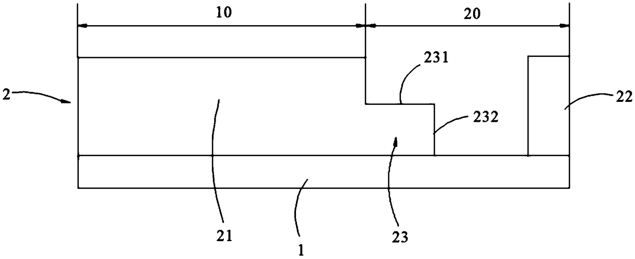
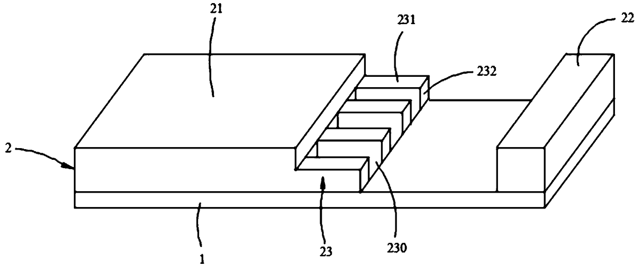
[0027] refer to figure 1 , figure 2 , the liquid crystal display of this embodiment has a display area 10 and a non-display area 20, and the non-display area 20 corresponds to the frame of the liquid crystal display. A liquid crystal display CF substrate, wherein the CF substrate includes a black matrix layer 1 and a color-resist layer 2, the color-resist layer 2 is arranged on the black matrix layer 1, and the color-resist layer 2 includes a first color-resist structure 21 and a second color-resist structure 22 , the second color-resisting structure 22 is disposed around the first color-resisting structure 21 and is spaced apart from the first color-resisting structure 21 . The color-resist layer 2 further includes a first step portion 23 protruding from the sidewall of the first color-resist structure 21 , and the first step portion 23 includes a portion extending from the sidewall of the first color-resist structure 21 toward the second color-resist structure 22 . The fi...
Embodiment 2
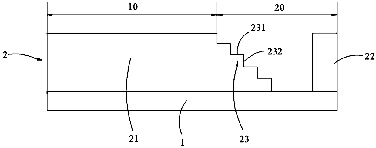
[0034] refer to image 3 , Figure 4 The difference between the CF substrate in this embodiment and the CF substrate in Embodiment 1 is that the number of first stepped portions 23 is at least two. The distances from the first stepped surfaces 231 of the at least two first stepped portions 23 to the black matrix layer 1 gradually decrease along the direction approaching the second color resist structure 22 .
[0035] At least two first stepped portions 23 correspond to the non-display area 20 of the liquid crystal display. In the alignment film printing process, the PI liquid dripped on the surface of the first color-resist structure 21 spreads to both sides, flows from the edge of the first color-resist structure 21 sequentially through at least two first steps 23, and then accumulates to the first color-resist structure. Between the resistance structure 21 and the second color resistance structure 22, when the PI liquid flows down from the edge of the first color resistanc...
Embodiment 3
[0040] refer to Figure 5 , Figure 6 The difference between the CF substrate in this embodiment and the CF substrate in Embodiment 2 is that the color-resist layer 2 further includes at least one second step portion 24 protruding inside the second color-resist structure 22, and the second step The portion 24 includes a third stepped surface 241 extending from the inner side of the second color-resisting structure 22 toward the first color-resisting structure 21 and a fourth stepped surface 242 extending from the third stepped surface 241 toward the black matrix layer 1, at least one The distance from the third stepped surface 241 of the second stepped portion 24 to the black matrix layer 1 gradually decreases along the direction approaching the first color resist structure 21 .
[0041] A plurality of second grooves 240 are arranged at intervals on the third step surface 241 of at least one second step portion 24 , and opening directions of the plurality of second grooves 24...
PUM
 Abstract
Description
Claims
Application Information


