A solar cell and a preparation method thereof
A solar cell and electrode technology, applied in the field of solar cells, can solve problems such as the reduction of open circuit voltage, the influence of passivation effect, the influence of solar cell conversion efficiency, etc., to achieve the effect of increasing open circuit voltage, reducing metal recombination rate, and improving virtual fill factor
- Summary
- Abstract
- Description
- Claims
- Application Information
AI Technical Summary
Problems solved by technology
Method used
Image

Examples
Embodiment 1
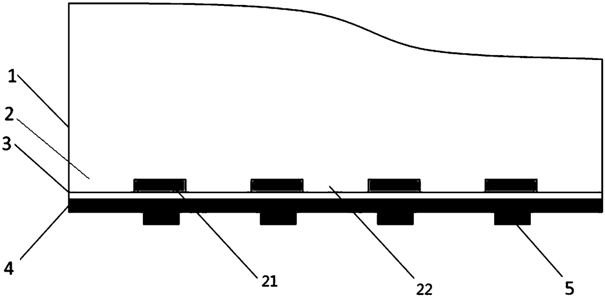
[0070] Such as figure 1 As shown, the solar cell provided by this embodiment includes a silicon substrate 1, and a selectively doped region 2 is arranged in the silicon substrate 1. The selectively doped region 2 includes a doped region 21 and an undoped region 22. The selectively doped A passivation medium layer 3 is provided on the surface of the impurity region 2 , a polysilicon film 4 is provided on the passivation medium layer 3 , and a metal contact electrode 5 is provided on the polysilicon film 4 at a position corresponding to the doped region 21 .
[0071] The polysilicon film 4 is a doped polysilicon film, and the doping element in the doped region 21 is the same as that in the doped polysilicon film, and the doping element is phosphorus.
[0072] The doping concentration of the doping element in the doping region 21 is 1.0E 18 atoms / cm 3 ~1.0E 20 atoms / cm 3 , The doping depth is 0.1-2 μm.
[0073] Doped regions 21 and non-doped regions 22 are alternately distri...
Embodiment 2
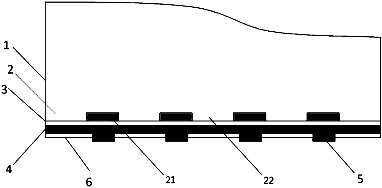
[0087] Such as figure 2 As shown, the solar cell provided by this embodiment includes a silicon substrate 1, and a selectively doped region 2 is arranged in the silicon substrate 1. The selectively doped region 2 includes a doped region 21 and an undoped region 22. The selectively doped A passivation dielectric layer 3 is provided on the surface of the impurity region 2, a polysilicon film 4 is provided on the passivation dielectric layer 3, a passivation layer 6 is also provided on the polysilicon film 4, and a passivation layer 6 is doped with A metal contact electrode 5 is provided at a position corresponding to the region 21 .
[0088] The polysilicon film 4 is a doped polysilicon film, and the doping element in the doped region 21 is the same as that in the doped polysilicon film, and the doping element is phosphorus.
[0089] The doping concentration of the doping element in the doping region 21 is 1.0E 18 atoms / cm 3 ~1.0E 20 atoms / cm 3 , The doping depth is 0.1-2 ...
Embodiment 3
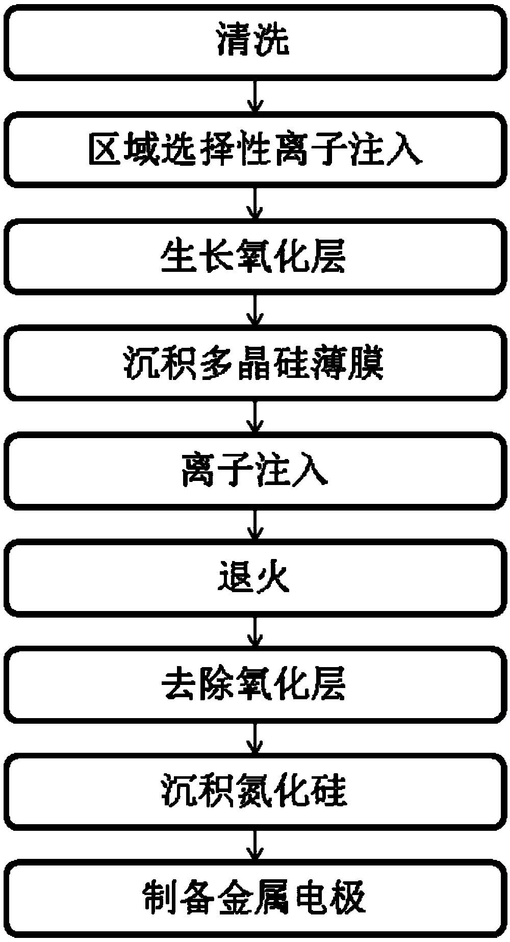
[0112] For the structure of the solar cell of this embodiment, refer to Embodiment 2.
[0113] The preparation method of the solar cell is based on chemical oxidation to prepare an ultra-thin oxide layer (SiO 2 ), the doping of the underlying silicon substrate is achieved by annealing after phosphorus implantation, and the entire process step requires separate annealing of the silicon substrate and polysilicon film doping.
[0114] Such as Figure 7 Shown, the preparation method of this solar cell specifically comprises the following steps:
[0115] A. Select the silicon substrate 1, after cleaning, use the mask plate (mask) that comes with the ion implanter to implant at one time, and the phosphorus (P) doping dose is 1E 15 atoms / cm 2 ;
[0116] B. Annealing: use a temperature of 900°C to activate the doped phosphorus (P) by furnace annealing to form a doped region 21 and a non-doped region 22;
[0117] C. Low-temperature furnace tube growth passivation medium layer: aft...
PUM
| Property | Measurement | Unit |
|---|---|---|
| Thickness | aaaaa | aaaaa |
| Thickness | aaaaa | aaaaa |
| Thickness | aaaaa | aaaaa |
Abstract
Description
Claims
Application Information
 - R&D Engineer
- R&D Manager
- IP Professional
- Industry Leading Data Capabilities
- Powerful AI technology
- Patent DNA Extraction
Browse by: Latest US Patents, China's latest patents, Technical Efficacy Thesaurus, Application Domain, Technology Topic.
© 2024 PatSnap. All rights reserved.Legal|Privacy policy|Modern Slavery Act Transparency Statement|Sitemap