Back-contact heterojunction solar cell and preparation method thereof

A solar cell and heterojunction technology, applied in circuits, photovoltaic power generation, electrical components, etc., can solve the problems of easy conduction, lower battery conversion efficiency, lower open circuit voltage and short circuit current, etc., achieve good repeatability, prevent leakage Current, the effect of increasing the open circuit voltage

Active Publication Date: 2016-04-20
TRINASOLAR CO LTD
View PDF2 Cites 8 Cited by
  • Summary
  • Abstract
  • Description
  • Claims
  • Application Information

AI Technical Summary

Problems solved by technology

However, the preparation of solar cells with this structure requires strict control of the entire process. The p-region and n-region of the p-n junction on the back of the cell are eas

Method used


Image

  • Back-contact heterojunction solar cell and preparation method thereof
  • Back-contact heterojunction solar cell and preparation method thereof
  • Back-contact heterojunction solar cell and preparation method thereof

Examples


Embodiment 1

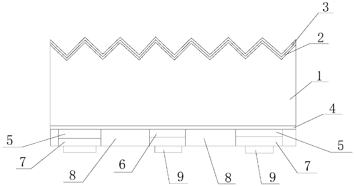
[0033] Such as figure 1 As shown, the full-back heterojunction solar cell of the present invention includes a silicon base layer 1, which is sequentially arranged on the front surface of the silicon base layer 1 N type The front surface field 2 and the antireflection layer 3 are provided with an intrinsic amorphous silicon passivation layer 4 on the back surface of the silicon base layer 1, and a P-type amorphous silicon layer is arranged at intervals on the intrinsic amorphous silicon passivation layer 4 5 and the N-type amorphous silicon layer 6, the P-type amorphous silicon layer 5 and the N-type amorphous silicon layer 6 are respectively provided with a transparent conductive film layer 7, and the transparent conductive film layer 7 is provided with an electrode. The thickness of the crystalline silicon layer 5 is 5-20nm, and the width is 100-1000μm; the thickness of the N-type amorphous silicon layer 6 is 5-20nm, and the width is 100-1000μm; The distance between the cen...

Embodiment 2

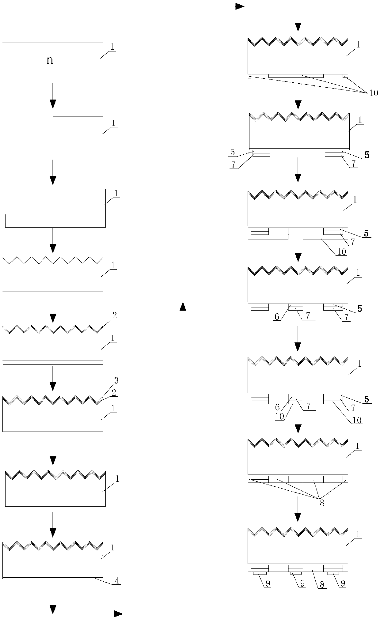
[0035] Such as figure 2 , image 3 As shown, taking the n-type silicon substrate as an example, the preparation method of the back contact heterojunction solar cell of the present invention comprises the following steps:

[0036] S1: providing a silicon wafer as the silicon base layer 1;

[0037] S2: Carry out standard RCA cleaning on the silicon base layer 1, and then use HF treatment to form a clean surface, rinse with deionized water and then blow dry;

[0038] S3: placing the silicon base layer 1 into a diffusion furnace, forming a silicon dioxide protective layer on the surface of the silicon base layer to protect the surface of the silicon wafer;

[0039] S4: Remove the silicon dioxide protective layer on one side, and form a pyramid structure on the front surface of the silicon substrate layer 1 through a single-side texturing process, followed by standard RCA cleaning;

[0040] S5: forming an N-type front surface field FSF2 on the pyramid structure through a diffus...


PUM

PropertyMeasurementUnit
Thicknessaaaaaaaaaa
Widthaaaaaaaaaa
Thicknessaaaaaaaaaa

Abstract

The invention discloses a full-back type heterojunction solar cell. The full-back type heterojunction solar cell comprises a silicon matrix layer and is characterized in that a front N-type surface field and an antireflection layer are sequentially arranged on the front surface of the silicon matrix layer, an intrinsic amorphous silicon passivation layer is arranged on the back surface of the silicon matrix layer, P-type amorphous silicon layers and N-type amorphous silicon layers are arranged on the intrinsic amorphous silicon passivation layer in a spaced manner, transparent conductive film layers are separately arranged on the P-type amorphous silicon layers and the N-type amorphous silicon layers, electrodes are arranged on the transparent conductive film layers, each P-type amorphous silicon layer has the thickness of 5-20nm and the width of 100-1,000 microns, each N-type amorphous silicon layer has the thickness of 5-20nm and the width of 100-1,000 microns, the center point of adjacent P-type amorphous silicon layers is spaced from the center point of the corresponding N-type amorphous silicon layer by 150-3,000 microns, and insulation isolating layers are arranged between the P-type amorphous silicon layers and the N-type amorphous silicon layers. The invention also discloses a preparation method of the full-back type heterojunction solar cell. According to the back-contact heterojunction solar cell and the preparation method thereof, the generation of leakage current can be prevented, and the open-circuit voltage of the solar cell is boosted.

Description

technical field [0001] The invention relates to a solar cell and a preparation method thereof, in particular to a back-contact heterojunction solar cell and a preparation method thereof, and belongs to the technical field of solar cell production. Background technique [0002] In recent years, the photoelectric performance of heterojunction cells has been greatly improved, and the conversion efficiency has reached 24.7%. In order to further improve the efficiency of traditional heterojunction cells, people have further improved the structure of heterojunction cells, and a heterojunction cell with a full back electrode structure has appeared, which can remove the shielding of the grid line from sunlight and increase the incidence of solar radiation. light absorption efficiency. At present, the highest efficiency of this full-back heterojunction solar cell has reached 25.6%. However, the preparation of solar cells with this structure requires strict control of the entire pro...

Claims


Application Information

Patent Timeline
IPC IPC(8): H01L31/072H01L31/0376H01L31/0352H01L31/0216H01L31/20
CPCH01L31/02168H01L31/0352H01L31/03762H01L31/072H01L31/202Y02E10/548Y02P70/50
Inventor 包健王栋良舒欣陈奕峰杨阳张学玲
Owner TRINASOLAR CO LTD
Why Eureka
Try Eureka