Shift register, driving method thereof and gate driving circuit
A shift register and gate technology, applied in static memory, digital memory information, instruments, etc., can solve the problems of insufficient discharge of the shift register, short charging time, and abnormal display of the display panel.
- Summary
- Abstract
- Description
- Claims
- Application Information
AI Technical Summary
Problems solved by technology
Method used
Image

Examples
Embodiment 1
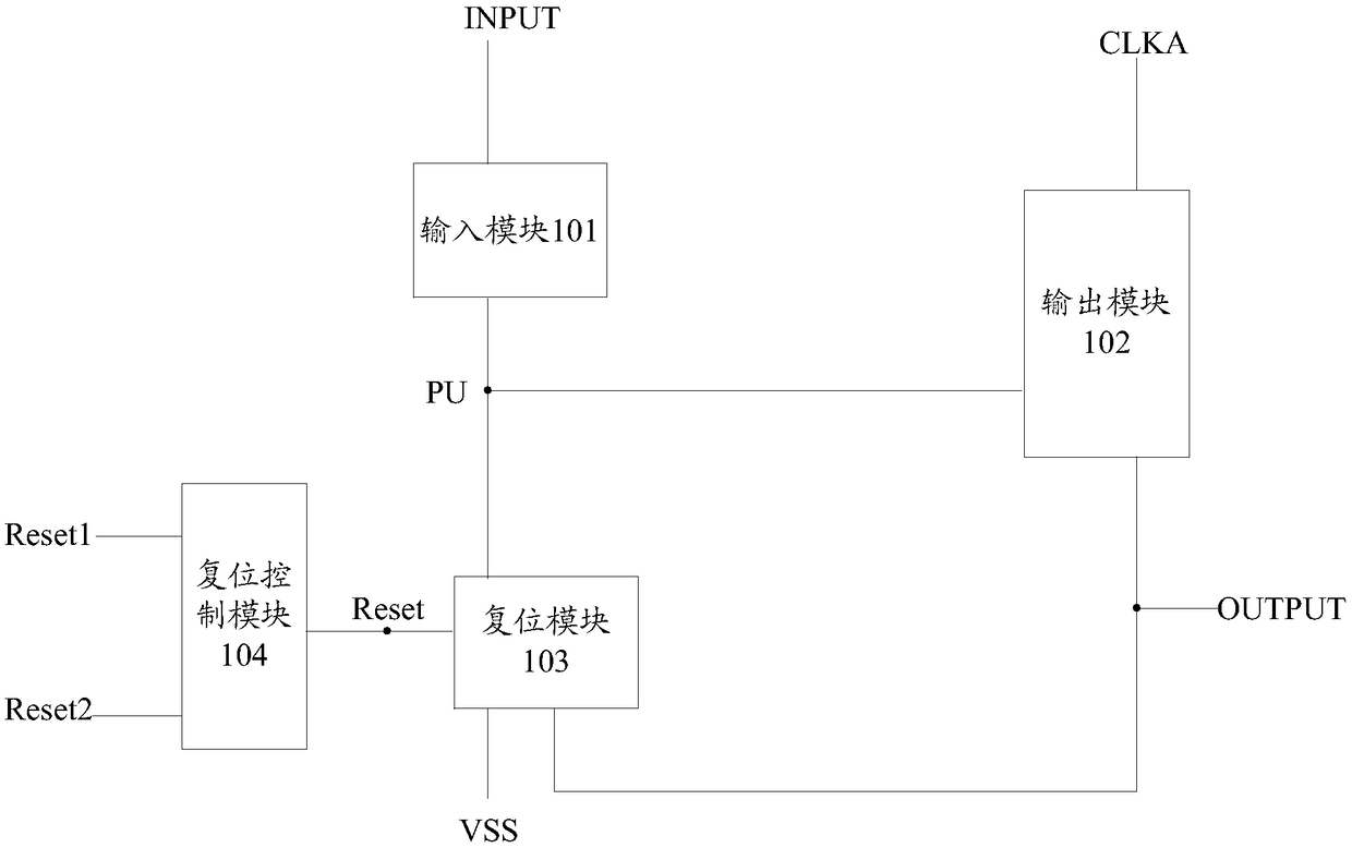
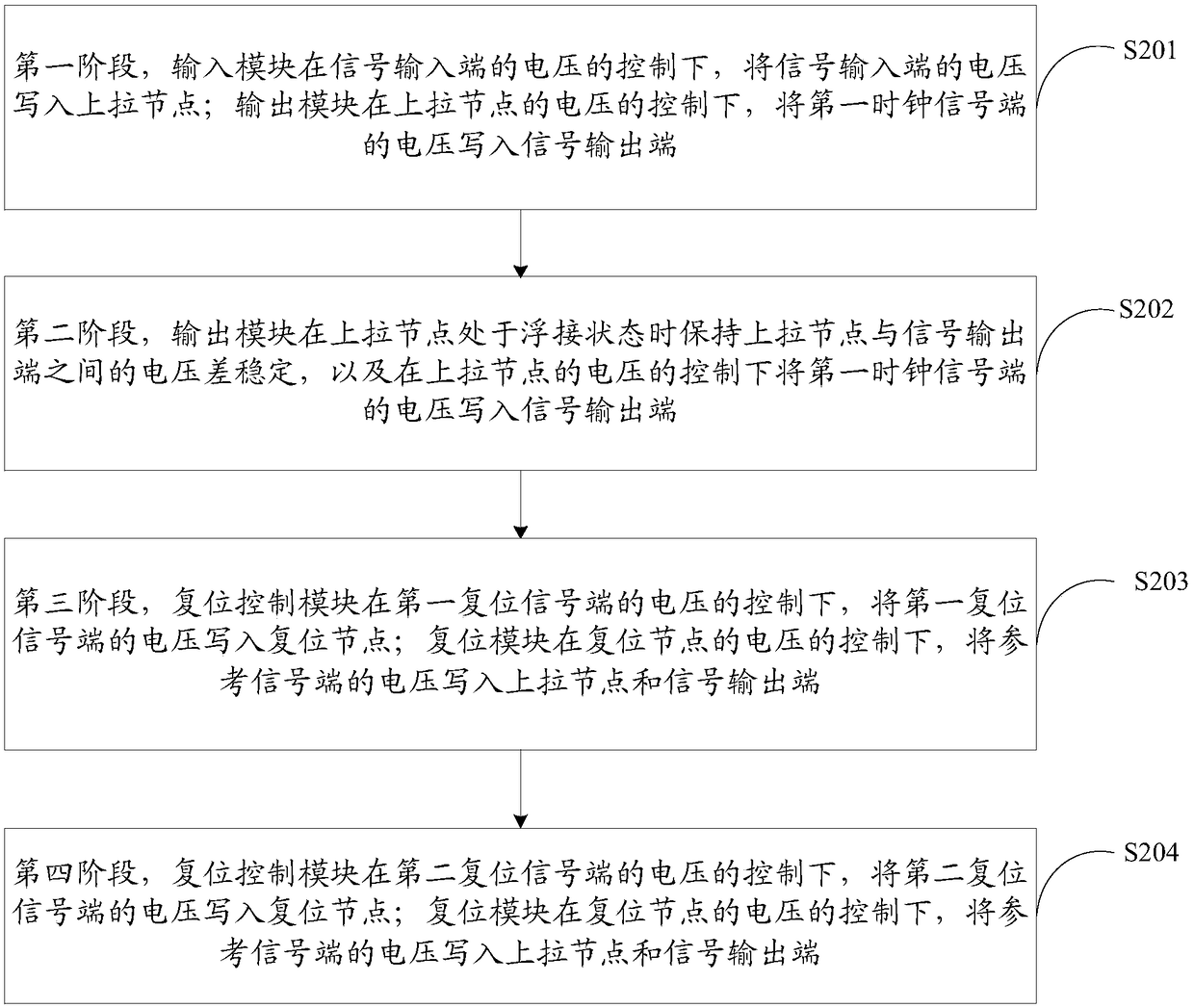
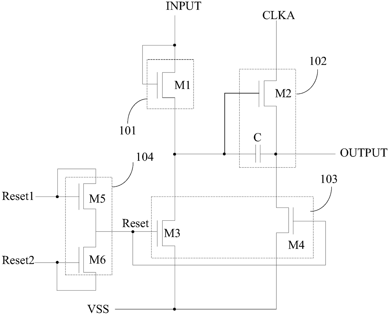
[0054] The first embodiment of the present invention provides a shift register, such as figure 1 As shown, it includes: an input module 101, an output module 102, a reset module 103 and a reset control module 104;
[0055] The input module 101 is respectively connected to the signal input terminal INPUT and the pull-up node PU, and is used for writing the voltage of the signal input terminal INPUT to the pull-up node PU under the control of the voltage of the signal input terminal INPUT;
[0056] The output module 102 is respectively connected to the first clock signal terminal CLKA, the pull-up node PU, and the signal output terminal OUTPUT, and is used to write the voltage of the first clock signal terminal CLKA to the signal output terminal under the control of the voltage of the pull-up node PU OUTPUT, and keep the voltage difference between the pull-up node PU and the signal output terminal OUTPUT stable when the pull-up node PU is in a floating state;
[0057] The reset module ...
Embodiment 2
[0085] The second embodiment of the present invention provides a shift register, such as Figure 5 As shown, it includes: an input module 101, an output module 102, a reset module 103, a reset control module 104, a pull-down control module 105, and a pull-down module 106;
[0086] The input module 101 is respectively connected to the signal input terminal INPUT and the pull-up node PU, and is used for writing the voltage of the signal input terminal INPUT to the pull-up node PU under the control of the voltage of the signal input terminal INPUT;
[0087] The output module 102 is respectively connected to the first clock signal terminal CLKA, the pull-up node PU, and the signal output terminal OUTPUT, and is used to write the voltage of the first clock signal terminal CLKA to the signal output terminal under the control of the voltage of the pull-up node PU OUTPUT, and keep the voltage difference between the pull-up node PU and the signal output terminal OUTPUT stable when the pull-u...
Embodiment 3
[0120] Based on the same inventive concept, the third embodiment of the present invention provides a gate driving circuit. Since the principle of the gate driving circuit to solve the problem is similar to that of the above-mentioned shift register, the third embodiment of the present invention provides the For the implementation of the gate driving circuit, reference may be made to the implementation of the above-mentioned shift register provided in the first and second embodiments of the present invention, and the repetitive parts will not be repeated.
[0121] Specifically, the gate driving circuit provided in the third embodiment of the present invention, such as Picture 9 As shown, it includes a plurality of cascaded shift registers provided in Embodiment 1 or 2 of the present invention;
[0122] The signal input terminal INPUT of the first stage shift register A1 is connected to the frame trigger signal terminal STA;
[0123] Except for the shift register A1 of the first stag...
PUM
 Abstract
Description
Claims
Application Information
 - R&D Engineer
- R&D Manager
- IP Professional
- Industry Leading Data Capabilities
- Powerful AI technology
- Patent DNA Extraction
Browse by: Latest US Patents, China's latest patents, Technical Efficacy Thesaurus, Application Domain, Technology Topic.
© 2024 PatSnap. All rights reserved.Legal|Privacy policy|Modern Slavery Act Transparency Statement|Sitemap