Panel defect analysis method, device and storage medium

A defect analysis and panel technology, applied in image analysis, image data processing, instruments, etc., can solve problems such as manpower consumption, misjudgment efficiency, and low efficiency, and achieve the effect of reducing workload and improving accuracy and efficiency

Active Publication Date: 2019-01-01
TENCENT TECH (SHENZHEN) CO LTD +1
View PDF7 Cites 34 Cited by
  • Summary
  • Abstract
  • Description
  • Claims
  • Application Information

AI Technical Summary

Problems solved by technology

[0004] During the research and practice of the existing technology, the inventors of the present invention found that the existing method only performs simple detection of specific defects, and subsequent evaluation and analysis by workers is required, due to the differences in subjective judgments of manual evaluation Misjudgments and inefficiencies caused by factors such as fatigue and fatigue, not only consume a lot of manpower, but also lead to very inaccurate and inefficient analysis results

Method used


Image

  • Panel defect analysis method, device and storage medium
  • Panel defect analysis method, device and storage medium
  • Panel defect analysis method, device and storage medium

Examples


Embodiment Construction

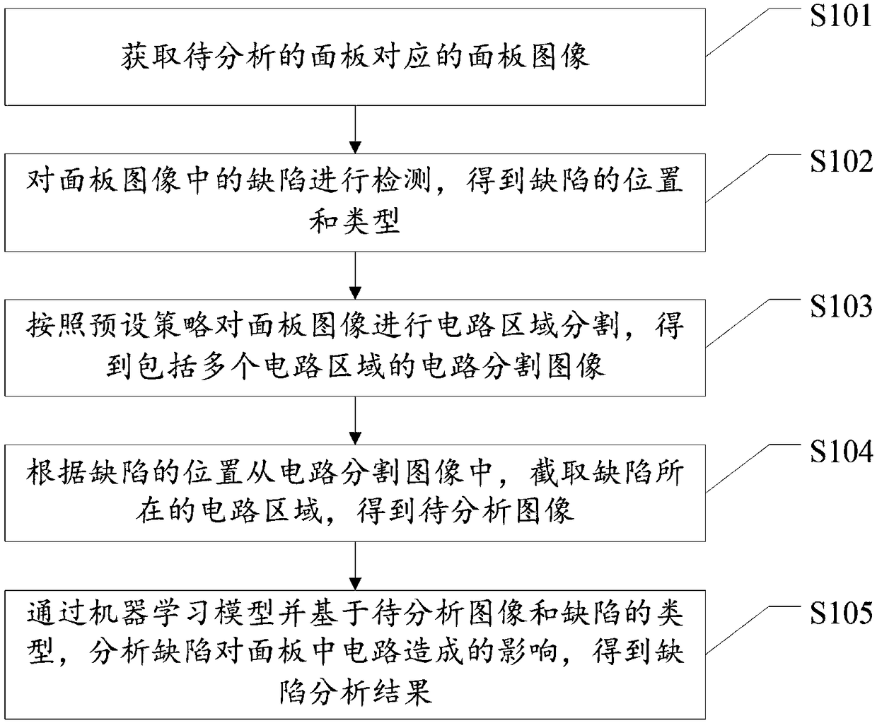
[0040] The following will clearly and completely describe the technical solutions in the embodiments of the present invention with reference to the accompanying drawings in the embodiments of the present invention. Obviously, the described embodiments are only some, not all, embodiments of the present invention. Based on the embodiments of the present invention, all other embodiments obtained by those skilled in the art without creative efforts fall within the protection scope of the present invention.

[0041] Embodiments of the present invention provide a panel defect analysis method, device and storage medium.

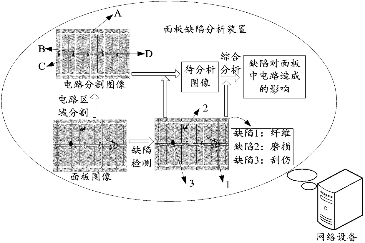
[0042] see figure 1 , figure 1 It is a schematic diagram of the scene of the panel defect analysis method provided by the embodiment of the present invention. The panel defect analysis method can be applied to a panel defect analysis device, and the panel defect analysis device can be integrated in a network device such as a terminal or a server. For example, The ...


PUM


Abstract

The embodiment of the invention discloses a panel defect analysis method, a device and a storage medium. The method comprises: obtaining a panel image corresponding to a panel to be analyzed; detecting defects in the panel image to obtain positions and types of defects; performing circuit region segmentation on the panel image according to a preset strategy to obtain a circuit segmented image including a plurality of circuit regions; according to the position of the defect, the circuit region where the defect being located is cut from the circuit segmentation image to obtain an image to be analyzed. A machine learn model is used to analyze that effect of the defect on the circuit in the panel based on the image to be analyzed and the type of the defect, and a defect analysis result is obtain. This scheme realizes the automatic detection and analysis of panel defects without the participation of workers, which not only reduces the manual workload, but also improves the accuracy and efficiency of panel defects analysis.

Description

technical field [0001] The invention relates to the technical field of panel detection, in particular to a panel defect analysis method, device and storage medium. Background technique [0002] Product quality is one of the most important production indicators in the manufacturing industry. In order to ensure product quality, defect detection of products has become an indispensable process in the production process. For example, thin film transistor liquid crystal displays (TFT-LCD, Thin Film Transistor -Liquid Crystal Display) as an example, each production line needs to perform defect inspection on TFT-LCD. [0003] In the prior art, in the process of defect detection of TFT-LCD, it is necessary to collect images of TFT-LCD, and use traditional image analysis methods to identify specific defects, so as to realize the judgment and detection of specific defect parts , and then manually evaluate and analyze the impact of the defect on the product and the product production p...

Claims


Application Information

Patent Timeline
Patent Type & Authority Applications(China)
IPC IPC(8): G06T7/00G06T7/11
CPCG06T7/0004G06T7/11G06T2207/20081G06T2207/20084G06T2207/30121
Inventor 冀永楠
Owner TENCENT TECH (SHENZHEN) CO LTD
Why Eureka
Try Eureka