Liquid crystal display panel and manufacturing method thereof

A technology for a liquid crystal display panel and a manufacturing method, applied in nonlinear optics, instruments, optics, etc., can solve the problems of reducing the risk of sealant peeling, weak adhesion between the sealant and the substrate, etc., and achieve the effect of reducing the risk of peeling

Inactive Publication Date: 2019-01-04
TCL CHINA STAR OPTOELECTRONICS TECH CO LTD
View PDF4 Cites 17 Cited by
  • Summary
  • Abstract
  • Description
  • Claims
  • Application Information

AI Technical Summary

Problems solved by technology

[0005] The purpose of the present invention is to provide a liquid crystal display panel, which can solve the problem of weak adhesion between the frame glue and the substrate due to the overlapping of the alignment film and the frame glue, and reduce the risk of peeling off the frame glue
[0006] The purpose of the present invention is also to provide a method for manufacturing a liquid crystal display panel, which can solve the problem of weak adhesion between the frame glue and the substrate due to the overlapping of the alignment film and the frame glue, and reduce the risk of peeling off the frame glue

Method used


Image

  • Liquid crystal display panel and manufacturing method thereof
  • Liquid crystal display panel and manufacturing method thereof
  • Liquid crystal display panel and manufacturing method thereof

Examples


Embodiment Construction

[0037] In order to further illustrate the technical means adopted by the present invention and its effects, the following describes in detail in conjunction with preferred embodiments of the present invention and accompanying drawings.

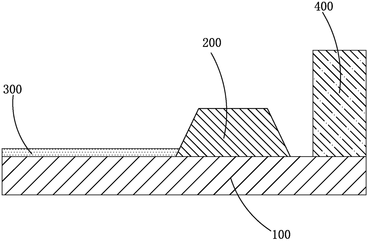
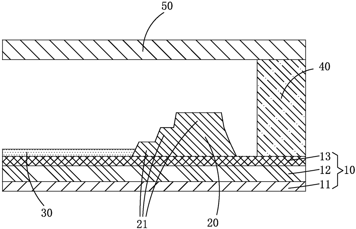
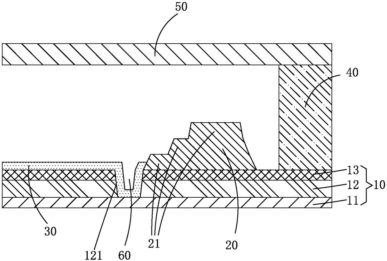
[0038] see figure 2 The first embodiment of the liquid crystal display panel of the present invention includes a first substrate 10 and a barrier wall 20 , an alignment film 30 and a sealant 40 disposed on the first substrate 10 . The retaining wall 20 is ring-shaped, the alignment film 30 is located inside the retaining wall 20 , and the sealant 40 is located outside the retaining wall. The retaining wall 20 includes at least two layers of sub-retaining walls 21 arranged sequentially from bottom to top. Each sub-retaining wall 21 is ring-shaped. Among the two adjacent sub-retaining walls 21, the vertical projection of the inner wall of the upper sub-retaining wall 21 is located between the inner side wall and the outer side wall of the low...


PUM


Abstract

The invention provides a liquid crystal display panel and a manufacturing method thereof. The liquid crystal display panel comprises a first substrate, a baffle wall, an alignment film and frame glue,wherein the baffle wall, the alignment film and the frame glue are arranged on the first substrate, the baffle wall is in an annular shape, the alignment film is arranged at an inner side of the baffle wall, the frame glue is arranged at an outer side of the baffle film, the baffle film comprises at least two layers of sub baffle walls which are sequentially arranged from bottom to top, each subbaffle wall is in an annular shape, in two adjacent layers of baffle walls, the projection of an inner side wall of the sub baffle wall at an upper layer is arranged between an inner side wall and anouter side wall of the sub baffle wall at a lower layer, so that the inner side wall of the baffle wall is in a step shape, the climbing resistance of a solution for forming the alignment film at theinner side wall of the baffle wall is greatly improved during preparation of the alignment film at the inner side of the baffle wall by a solution film formation mode, the alignment film is preventedfrom being expanded out of the baffle plate and overlapped with the frame glue, and the stripping risk of the frame glue is reduced.

Description

technical field [0001] The invention relates to the field of display technology, in particular to a liquid crystal display panel and a manufacturing method thereof. Background technique [0002] With the development of display technology, liquid crystal display (Liquid Crystal Display, LCD) and organic light emitting diode display (Organic Light Emitting Diode, OLED) and other flat display devices have high image quality, power saving, thin body and wide application range, etc. Advantages, and are widely used in various consumer electronics products such as mobile phones, televisions, personal digital assistants, digital cameras, notebook computers, desktop computers, etc., and become the mainstream of display devices. [0003] Most of the liquid crystal displays currently on the market are backlight liquid crystal displays, which include a liquid crystal display panel and a backlight module. The working principle of the liquid crystal display panel is to pour liquid crysta...

Claims


Application Information

Patent Timeline
Patent Type & Authority Applications(China)
IPC IPC(8): G02F1/1339G02F1/1337G02F1/1333
CPCG02F1/1333G02F1/1337G02F1/1339
Inventor 衣志光
Owner TCL CHINA STAR OPTOELECTRONICS TECH CO LTD
Why Eureka
Try Eureka