
Semiconductor integrated circuit device

An integrated circuit and semiconductor technology, which is applied in the field of power cutoff, can solve the problems of reduced degree of freedom in layout, poor timing convergence, and increased design man-hours, and achieve the effect of suppressing voltage drop

Active Publication Date: 2019-01-04
SOCIONEXT INC
View PDF15 Cites 5 Cited by
  • Summary
  • Abstract
  • Description
  • Claims
  • Application Information

AI Technical Summary

Problems solved by technology

In other words, there may be a problem of increased design man-hours due to the increase in area due to the presence of many switches and the decrease in the degree of freedom in standard cell layout, resulting in poor timing convergence.

Method used


Image

  • Semiconductor integrated circuit device
  • Semiconductor integrated circuit device
  • Semiconductor integrated circuit device

Examples


no. 1 approach

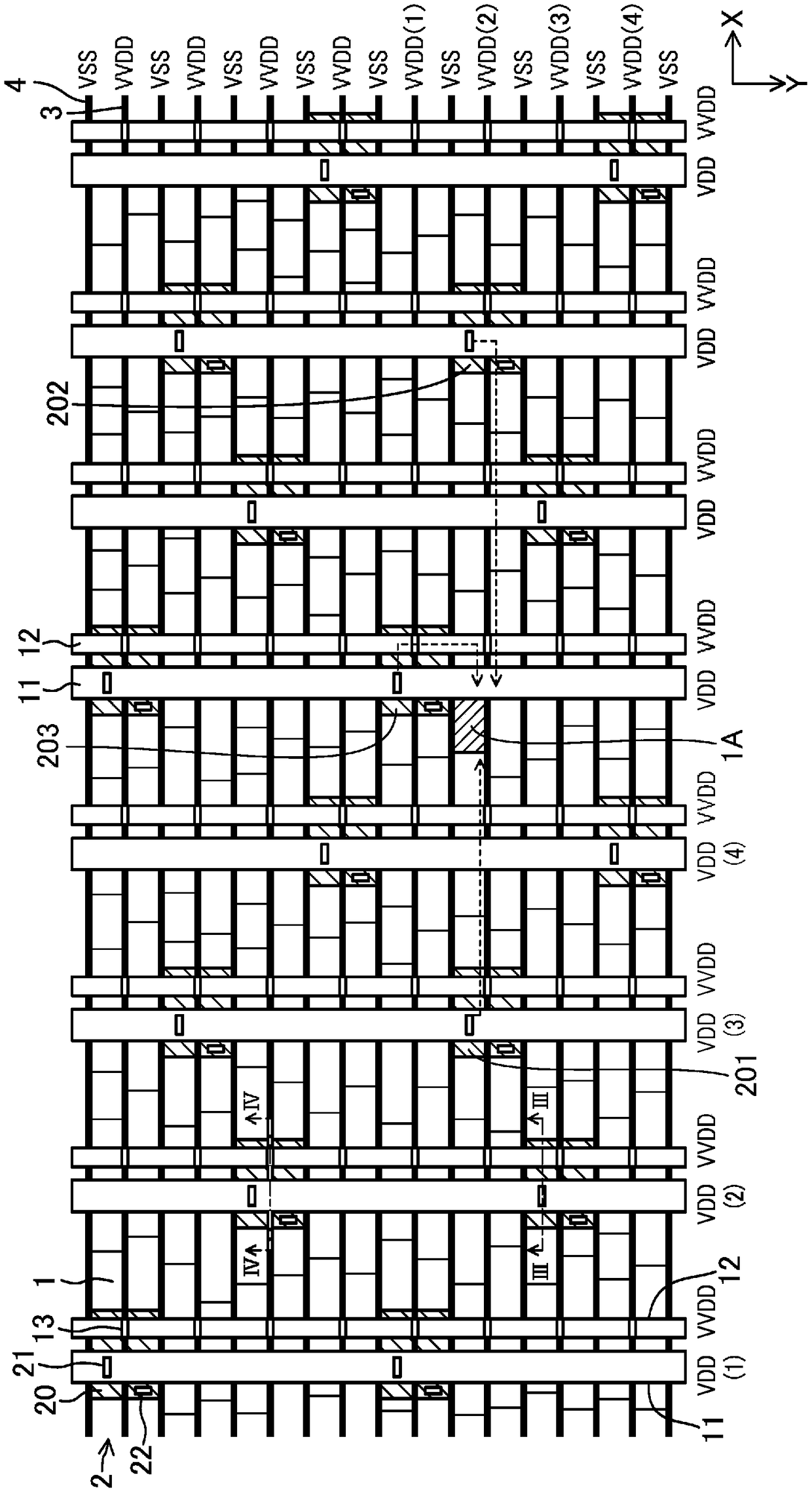
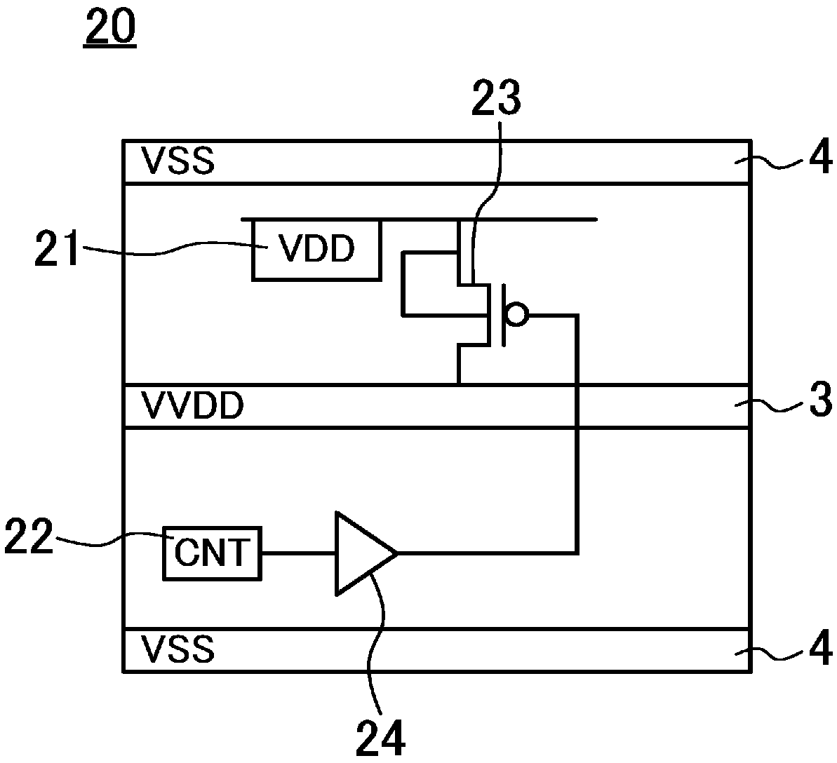
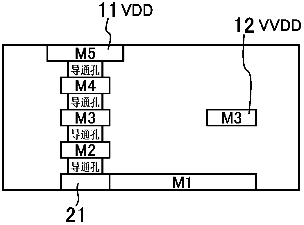
[0032] figure 1 It is a plan view showing the configuration of the semiconductor integrated circuit device according to the first embodiment, and it shows a simplified layout pattern in a circuit block to be powered off (the same applies to the plan views below). exist figure 1 In the illustrated semiconductor integrated circuit device, a plurality of standard cells 1 are arranged on a substrate. The standard cell row 2 has a plurality of standard cells 1 arranged side by side along the X direction (the horizontal direction of the drawing, which is equivalent to the first direction), and the standard cell row 2 is along the Y direction (the vertical direction of the drawing, which is the direction perpendicular to the first direction, that is, the first direction). Two directions) are arranged in multiple rows. The standard cell 1 is a basic circuit element having functions such as an inverter, a logic circuit, etc., and by arranging and wiring the standard cells 1 in combin...

Deformed example 1

[0047] exist figure 1 In the structure of the four strip-shaped power supply wiring 11 (1) ~ (4), the four strip-shaped power supply wiring 11 (1) ~ (4) and the standard unit power supply wiring 3 (1), (3), ( Between 2) and (4), a switch unit 20 is sequentially arranged. However, the layout pattern of the switch unit 20 is not limited to figure 1 pattern shown.

[0048] Figure 5 It is a plan view showing the configuration of a semiconductor integrated circuit device according to Modification 1 of the present embodiment. The layout of the standard cell 1, the layout of the standard cell power supply wiring 3, the ground power supply wiring 4, the strip power supply wiring 11, and the sub strip power supply wiring 12 and figure 1 Same, not detailed here.

[0049] and figure 1 The composition of the same, in Figure 5 In the configuration, one switching unit 20 is arranged for every four standard cell power supply wirings 3 for each strip-shaped power supply wiring 11 . ...

Deformed example 2

[0053] Figure 6 It is a plan view showing the configuration of a semiconductor integrated circuit device according to Modification 2 of the present embodiment. exist Figure 6 In , for simplification of the illustration, the illustration about the arrangement of the standard cell 1 is omitted. Also, the arrangement of the standard cell power supply wiring 3, the ground power supply wiring 4, the strip power supply wiring 11, and the sub strip power supply wiring 12 is basically the same as figure 1 Same, not detailed here.

[0054] exist Figure 6 In the configuration of , the size of the switch unit 25 in the Y direction, that is, the unit height is figure 1 Twice the height of the switch cell 20, equal to the height of the column 2 of four standard cells. Furthermore, each switching unit 25 is provided between the strip-shaped power supply wiring 11 and the two standard cell power supply wirings 3 . That is, when two standard cell power supply wirings 3 are regarded a...


PUM


Abstract

Switch cells (20) are provided in a circuit block having standard cells (1) arranged therein, said switch cells being capable of switching between electrical connection and disconnection of power supply wires (3) extending in the X direction and strap power supply wires (11) extending in the Y direction. One switch cell (20) is arranged on the strap power supply wires (11) for every M number (M being an integer of at least 3) of power supply wires (3). The switch cell (20) arrangement positions in the Y direction differ from each other in adjacent strap power supply wires (11) and are the sameat every M number of strap power supply wires (11) in the X direction.

Description

technical field [0001] The present disclosure relates to a power cutoff technique in a semiconductor integrated circuit device. Background technique [0002] One of technologies for realizing low power consumption of semiconductor integrated circuit devices is a power cutoff technology. The power cut-off technology is a technology that divides the inside of a semiconductor integrated circuit device into a plurality of circuit blocks and cuts off the power supply of the circuit blocks that are not operating, thereby suppressing leakage current that is a cause of power consumption. Patent Document 1 discloses a configuration in the field of power cutoff in which a switch for power supply / cutoff is arranged in each standard cell column to realize power supply control. Power is supplied to each standard cell from the strip power supply wiring via the switch and the standard cell power supply wiring. [0003] Patent Document 1: Japanese Laid-Open Patent Publication No. 2008-277...

Claims


Application Information

Patent Timeline
IPC IPC(8): H01L21/822G06F1/26H01L21/82H01L27/04
CPCH01L2027/11881H01L27/11807H01L23/5286H01L27/0207H03K19/0016G06F30/392G06F30/394G06F30/39G06F1/26
Inventor 冈本淳北浦智靖武野纮宜
Owner SOCIONEXT INC
Learn More