A chip packaging structure and a chip packaging method

A chip packaging structure and chip packaging technology, which is applied to electrical components, electrical solid devices, circuits, etc., can solve the problems of poor chip packaging effects, and achieve good results and firm and reliable electrical connections

Pending Publication Date: 2019-01-11
CHINA WAFER LEVEL CSP
View PDF0 Cites 2 Cited by
  • Summary
  • Abstract
  • Description
  • Claims
  • Application Information

AI Technical Summary

Problems solved by technology

[0005] In view of this, an embodiment of the present invention provides a chip packaging structure and

Method used


Image

  • A chip packaging structure and a chip packaging method
  • A chip packaging structure and a chip packaging method
  • A chip packaging structure and a chip packaging method

Examples


Embodiment Construction

[0067] In order to make the purpose, technical solution and advantages of the present invention clearer, the technical solution of the present invention will be fully described below through specific implementation in combination with the drawings in the embodiments of the present invention. Apparently, the described embodiments are some embodiments of the present invention, rather than all embodiments. Based on the embodiments of the present invention, all other embodiments obtained by persons of ordinary skill in the art without making creative efforts, All fall within the protection scope of the present invention.

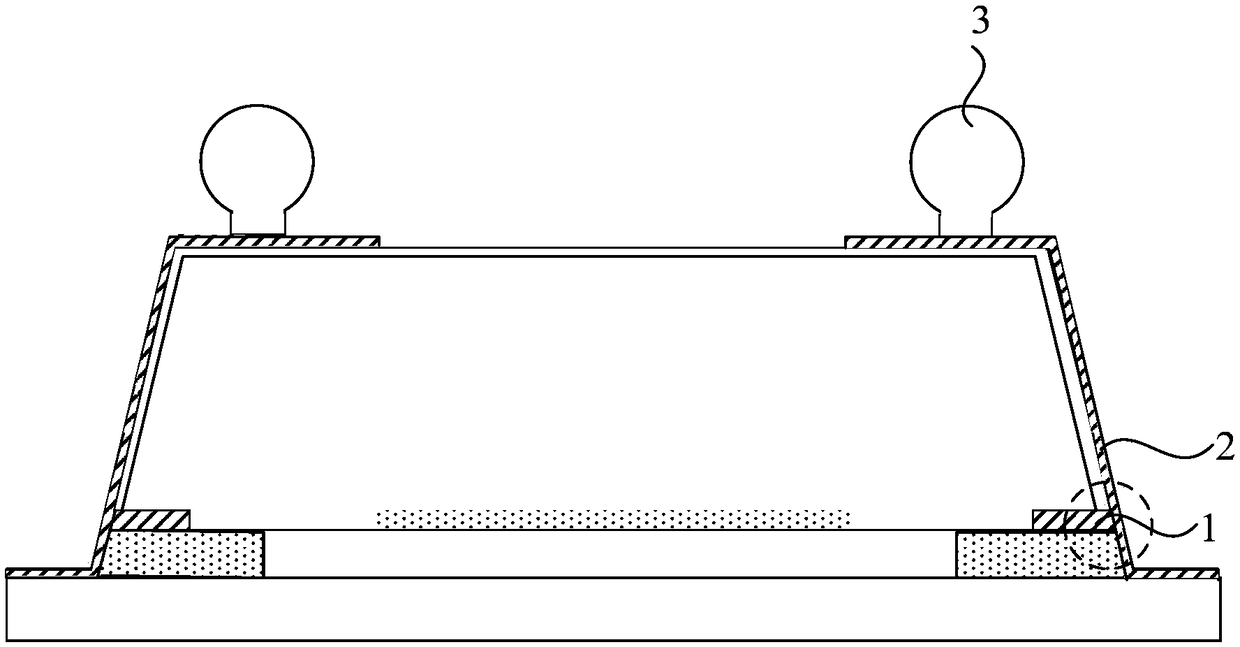
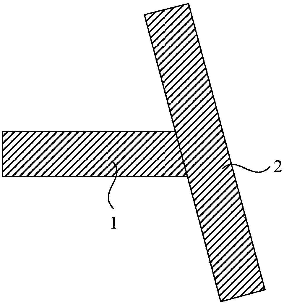
[0068] figure 1 is a structural schematic diagram of a chip packaging structure in the prior art, figure 2 yes figure 1 The enlarged schematic diagram of the provided chip package structure in area A, such as figure 1 and figure 2 As shown, the pad 1 on the chip is electrically connected to the metal solder ball 3 through the metal wiring 2, and the metal ...


PUM


Abstract

The invention discloses a chip packaging structure and a chip packaging method. The chip packaging structure comprises a substrate, a component region and a bonding pad arranged on the first side of the substrate. The bonding pad is located on the outside of the component region and is electrically connected with the component in the component region. An insulating layer covering a second surfaceof the substrate and a side wall, wherein a first via hole is formed on the insulating layer to expose a part of the back surface of the solder pad; a rewiring layer located on the insulating layer and extending from the second side along the sidewall into the first via of the insulating layer and extending outwardly to the side of the solder pad to electrically connect with a back surface of a portion of the solder pad exposed by the first via and a side surface of the solder pad; a solder bump is formed on the second surface of the substrate and is electrically connected to the rewiring layer. By adopting the technical proposal, the contact area between the rewiring layer and the bonding pad can be increased, the connection reliability between the rewiring layer and the bonding pad can be improved, and the good packaging effect of the chip packaging structure can be ensured.

Description

technical field [0001] Embodiments of the present invention relate to the technical field of wafer-level chip packaging, and in particular, to a chip packaging structure and a chip packaging method. Background technique [0002] The development trend of electronic equipment is miniaturization and portability. A major factor determining the miniaturization and portability of electronic equipment is the packaging design of chips in electronic equipment. The traditional chip packaging method usually uses wire bonding (Wire Bonding) for packaging, but with the rapid development of integrated circuits, longer leads make the product size unable to meet the ideal requirements. Therefore, wafer level packaging (Wafer Level Package, WLP) has gradually replaced wire-bonded packaging as a more commonly used packaging method. [0003] Wafer-level packaging technology is a technology that performs packaging and testing on the entire wafer and then cuts it into individual chips. The siz...

Claims


Application Information

Patent Timeline
IPC IPC(8): H01L23/31H01L23/498H01L21/56
CPCH01L23/49816H01L21/561H01L23/3128H01L2224/11
Inventor 王之奇谢国梁陈立行
Owner CHINA WAFER LEVEL CSP
Why Eureka
Try Eureka