Display panel, manufacturing method thereof, and display device

A display panel and display device technology, which is applied in semiconductor/solid-state device manufacturing, semiconductor devices, electrical components, etc., can solve the problems of large parallel resistance between the cathode and auxiliary cathode, and the influence of the display effect of the display panel, so as to increase the contact area, Reduce the resistance and ensure the effect of display effect

Active Publication Date: 2021-01-26
BOE TECH GRP CO LTD +1
View PDF14 Cites 0 Cited by
  • Summary
  • Abstract
  • Description
  • Claims
  • Application Information

AI Technical Summary

Problems solved by technology

[0005] Embodiments of the present invention provide a display panel, a manufacturing method thereof, and a display device, which can solve the problem in the related art that the parallel resistance of the cathode and the auxiliary cathode is relatively large, and the display effect of the display panel will be affected.

Method used


Image

  • Display panel, manufacturing method thereof, and display device
  • Display panel, manufacturing method thereof, and display device
  • Display panel, manufacturing method thereof, and display device

Examples


Embodiment Construction

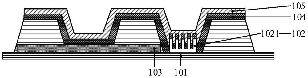
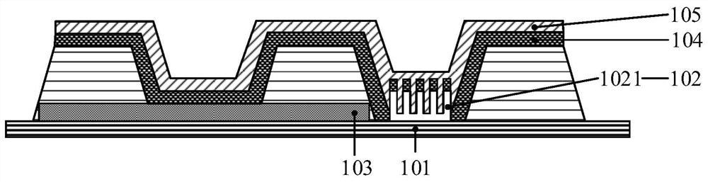
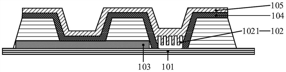
[0043] In order to make the object, technical solution and advantages of the present invention clearer, the implementation manner of the present invention will be further described in detail below in conjunction with the accompanying drawings.

[0044] In recent years, due to the advantages of high color saturation and flexibility and deformability of flexible OLED display panels, their applications have become more and more widespread. As the screen of the display panel increases, the area of ​​the pixel unit on the display panel increases accordingly. Moreover, the potential drop caused by the resistance of the cathode tends to be significant, resulting in a decrease in the voltage difference between the anode and the cathode, thereby causing a brightness gradient to appear in the display area of ​​the display panel. For example, for a top-emission display panel, in order to ensure the transmittance of the electrode (cathode) on the light-emitting side, and because the elect...


PUM


Abstract

The invention discloses a display panel, a manufacturing method thereof, and a display device, belonging to the technical field of display. The display panel includes: an auxiliary cathode layer and an anode layer arranged on a base substrate, and a light-emitting layer and a cathode layer stacked on the base substrate provided with the anode layer, the anode layer and the anode layer The auxiliary cathode layer is insulated; the auxiliary cathode layer includes at least one auxiliary cathode structure, and each of the auxiliary cathode structures is provided with at least one groove on the surface away from the base substrate, and the cathode layer is in the groove in contact with the auxiliary cathode layer. The invention increases the contact area between the auxiliary cathode and the cathode layer, reduces the parallel resistance between the auxiliary cathode structure and the cathode layer, achieves the effect of reducing the resistance of the cathode structure, and effectively ensures the display effect of the display panel. The invention is used to display images.

Description

technical field [0001] The present invention relates to the field of display technology, in particular to a display panel, a manufacturing method thereof, and a display device. Background technique [0002] An organic light-emitting diode (English: Organic Light-emitting Diode; abbreviation: OLED) display panel may include an anode, a pixel defining layer, an organic light-emitting layer, and a cathode. Wherein, the brightness of the organic light-emitting layer can be controlled by the voltage difference formed between the cathode and the anode. However, when the resistance of the cathode is large, the cathode has a significant impact on the voltage difference, resulting in a brightness gradient in the display of the display panel. [0003] In the related art, the function of the original cathode can be replaced by setting a cathode structure, the cathode structure includes: a parallel cathode and an auxiliary cathode, and the auxiliary cathode is made of metal. The resis...

Claims


Application Information

Patent Timeline
Patent Type & Authority Patents(China)
IPC IPC(8): H01L51/52H01L51/56H01L27/32
CPCH10K59/12H10K50/824H10K71/00
Inventor 张振华黎恩源全盛
Owner BOE TECH GRP CO LTD
Why Eureka
Try Eureka