Array substrate and display device

A technology for array substrates and conductive parts, which is applied in the field of array substrates and display devices, and can solve problems such as fracture, affecting signal transmission, and electrostatic breakdown

Active Publication Date: 2019-01-25
BOE TECH GRP CO LTD +1
View PDF3 Cites 4 Cited by
  • Summary
  • Abstract
  • Description
  • Claims
  • Application Information

AI Technical Summary

Problems solved by technology

Since the projections of the two layers of signal lines 11 and 12 on the substrate are relatively arranged but do not overlap each other, when the signal line 11 or 12 is loaded with an electrical signal, a large amount of electricity will be accumulated at the ends of the two signal lines 11 and 12 that are close to each other. Electrostatic

Method used


Image

  • Array substrate and display device
  • Array substrate and display device
  • Array substrate and display device

Examples


Example Embodiment

[0042] Example one

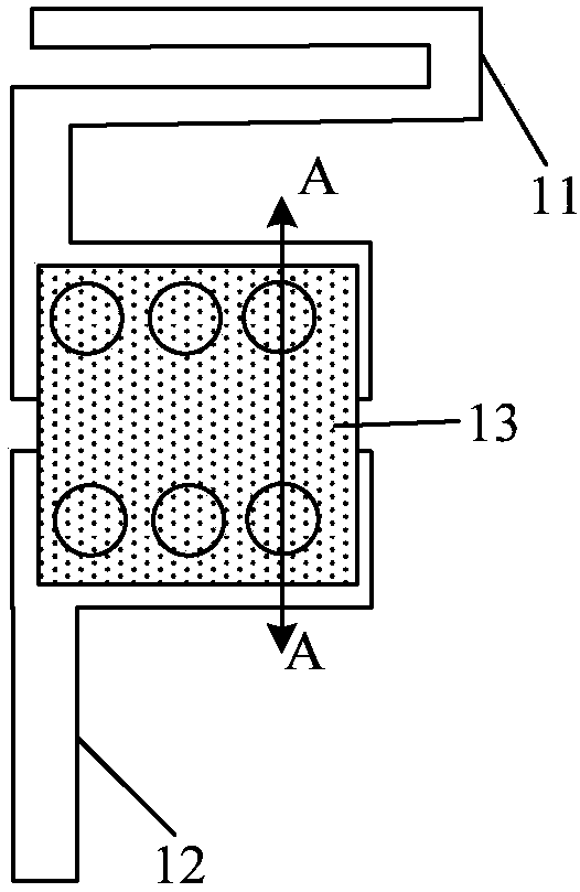
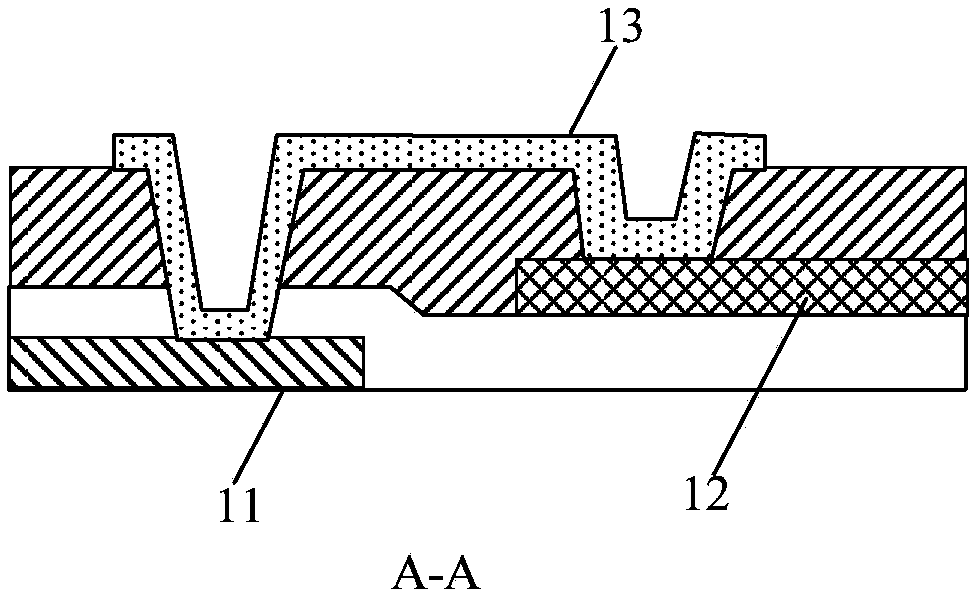
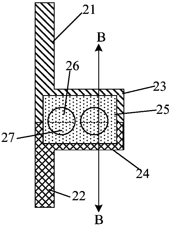
[0043] Specifically, the first connection mode of the first conductive portion 23 and the second conductive portion 24 is as follows: image 3 with Figure 4 As shown, a part (about half) of the orthographic projection of the first conductive portion 23 on the substrate 20 is located within the orthographic projection range of the second conductive portion 24 on the substrate 20, and the other portion is located within the orthographic projection of the second conductive portion 24 on the substrate 20. Outside the orthographic projection on the substrate 20. The orthographic projection of the second via 27 on the substrate 20 is within the range of the orthographic projection of the second conductive portion 24 on the substrate 20, and the orthographic projection of the first via 26 on the substrate 20 is located on the second conductive portion 24. The orthographic projection range on the substrate 20 is outside, and the orthographic projection of each first...

Example Embodiment

[0044] Example two

[0045] The second connection mode of the first conductive portion 23 and the second conductive portion 24 is as follows: Figure 5 with Image 6 As shown, most or all of the orthographic projection of the first conductive portion 23 on the substrate 20 is located within the orthographic projection range of the second conductive portion 24 on the substrate 20. The second conductive portion 24 includes at least one slit 241 penetrating the second conductive portion 24. The orthographic projection of the first via 26 on the substrate 20 is within the orthographic projection range of the slit 241 on the substrate 20. The projection of the via 27 on the substrate is outside the range of the orthographic projection of the slit 241 on the substrate 20, and the orthographic projection of each first via 26 and the orthographic projection of the corresponding second via 27 do not overlap and are mutually exclusive. Adjacent. with Figure 4 The setting method in is sim...

Example Embodiment

[0048] Example three

[0049] The third connection mode of the first conductive portion 23 and the second conductive portion 24 is as follows Figure 7 with Picture 8 As shown, in order to clearly see the structure of the first conductive portion 23 and the second conductive portion 24 and the connection relationship between the two, in Figure 7 The middle connection structure 25 is represented by a transparent film layer without pattern filling. The first conductive portion 23 includes a first comb handle portion 23a and a plurality of spaced first comb tooth portions 23b connected to the first comb handle portion 23a. The area where the first conductive portion 23 is located is the first comb handle portion 23a, The plurality of first comb-tooth portions 23b and the sum of the regions where the intervals between the first comb-tooth portions 23b are located. The second conductive portion 24 includes a second comb handle portion 24a and a plurality of spaced second comb tooth ...


PUM


Abstract

The invention provides an array substrate. The array substrate comprises a first signal line and a second signal line which are arranged on different insulated and spaced layers of a substrate; one end of the first signal line comprises a first conductive part; one end of the second signal line comprises a second conductive part; the first conductive part and the second conductive part are electrically connected through a connecting structure; and the orthographic projections of an area where the first conductive part is located and an area where the second conductive part is located, on the substrate, are at least partially overlapped. Correspondingly, the invention further provides a display device. According to the array substrate, the disconnection between the signal lines can be reduced, so that the effect of connection between different signal lines can be improved.

Description

technical field [0001] The present invention relates to the field of display technology, in particular to an array substrate and a display device. Background technique [0002] In the manufacturing process of the display device, in order to meet the electrical connection between different layers of signal lines, it is often necessary to set up a transfer structure around the display panel, that is, to set a via hole on the insulating layer between the two layers of signal lines. Connection structures such as indium tin oxide (ITO) connect the two layers of signal lines, and the design of the transfer point directly affects the quality of the electrical connection. [0003] figure 1 It is the connection schematic diagram of the existing two-layer signal line transfer point, figure 2 yes figure 1 Sectional view along line AA. Since the projections of the two layers of signal lines 11 and 12 on the substrate are relatively arranged but do not overlap each other, when the s...

Claims


Application Information

Patent Timeline
IPC IPC(8): G02F1/1362G09F9/00
CPCG02F1/136204G02F1/136286G09F9/00G02F1/13629H01L23/50H01L27/12G02F1/13458G02F2201/506G09G3/20G09G2300/0426H01L27/1244
Inventor 李琳徐彦彬
Owner BOE TECH GRP CO LTD
Why Eureka
Try Eureka