
Eureka
For R&D, Eureka makes reading and utilizing patents & technical documents easy.
Eureka AIR
Designed for self-driven R&D workflows. Generate viable solutions, solve complex R&D challenges, empower your innovation with AI.

Eureka Materials
Designed for material experts only. Revolutionize your material R&D, from search, analyze, to developing new materials.

TechResearch
Generate reliable direction feasibility study reports for your R&D in just a few steps.

TechSeek
Discover and master advanced knowledge NOW. Basics, ideas, possibilities, all at once.

TechMind
As an expert in R&D Theories, TechMind can generates customized viable solutions instantly.

TechRisk
Analyze your overall solution with one click, know your potential R&D risks in advance.

TechMonitor
Get weekly tech updates, stay abreast of the latest tech innovations and key insights.
A defect detection method for PCB
A defect detection, PCB board technology, applied in image data processing, instrument, character and pattern recognition, etc., can solve problems such as low gray value and missed detection.
- Summary
- Abstract
- Description
- Claims
- Application Information
AI Technical Summary
Problems solved by technology
Method used
Image

Examples
Embodiment Construction
[0064] The present invention will be further described below in conjunction with the accompanying drawings and embodiments.
[0065] For the defect detection method of PCB, the steps are as follows:
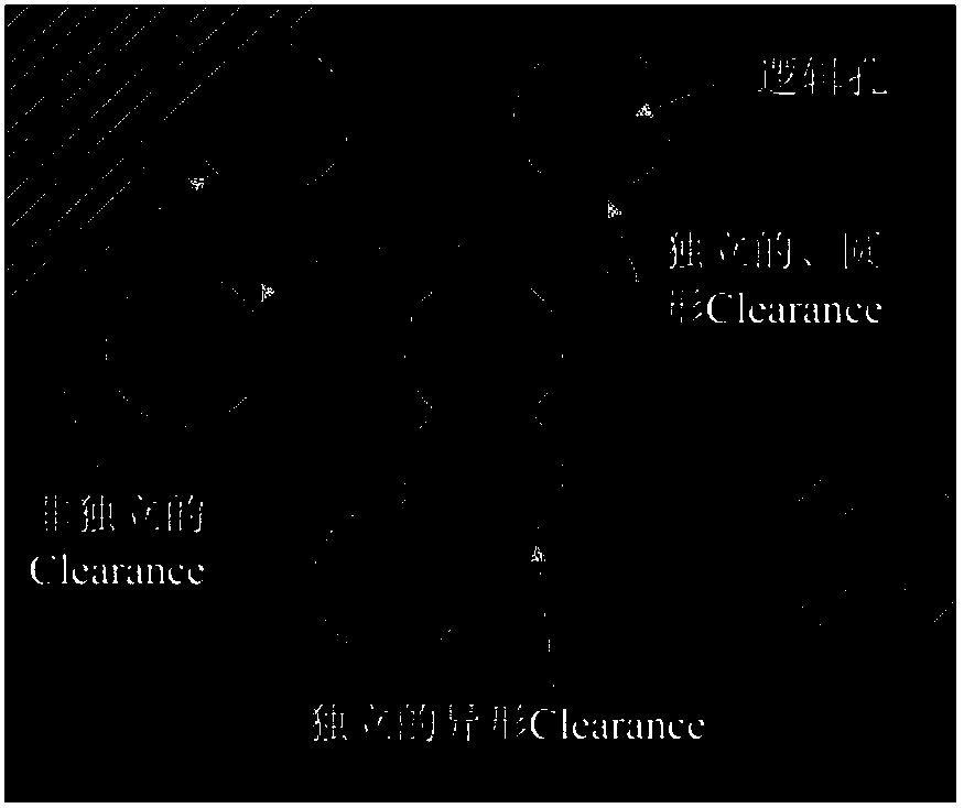
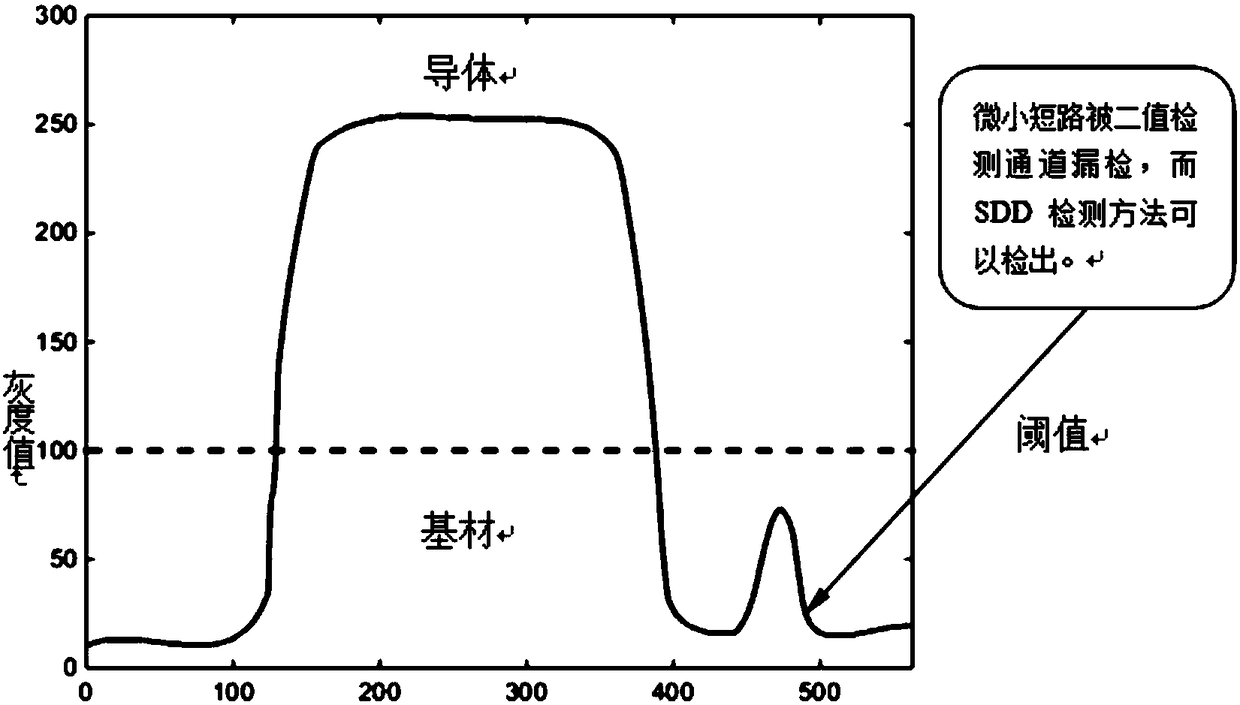
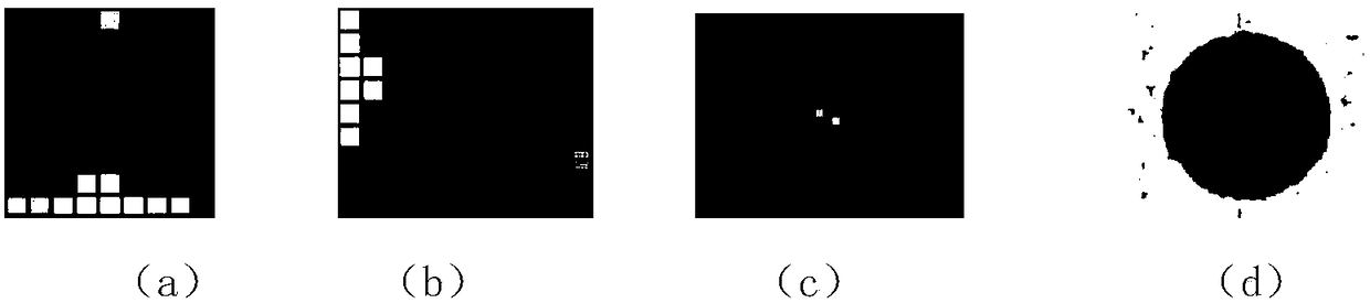
[0066] The tiny defects of the PCB board are divided into micro short circuits, micro burrs and isolated defects according to the number of connected conductors, such as image 3 , wherein the tiny short circuit means a tiny defect connecting two conductors, the tiny burr means a tiny defect connecting a conductor, and the isolated defect means a tiny defect not connecting a conductor. For the first two types, the tiny short circuit and tiny burr will affect the electrical conductivity of the PCB board, so it needs to be detected, and for the isolated defect that is not connected to the conductor, it needs to be judged whether it is a blank area inside the clearance, if it is located In the blank area, the isolated defects located in the blank area need to be detected, while the...
PUM
 Abstract
Description
Claims
Application Information
 - R&D Engineer
- R&D Manager
- IP Professional
- Industry Leading Data Capabilities
- Powerful AI technology
- Patent DNA Extraction
Browse by: Latest US Patents, China's latest patents, Technical Efficacy Thesaurus, Application Domain, Technology Topic, Popular Technical Reports.
© 2024 PatSnap. All rights reserved.Legal|Privacy policy|Modern Slavery Act Transparency Statement|Sitemap|About US| Contact US: help@patsnap.com