Flash memory structure and corresponding programming, erasing and reading methods

A flash memory, erasing voltage technology, applied in the semiconductor field, can solve the problems of small process window, small erasing saturation process window, small capacitive coupling coefficient, etc., and achieve the effect of avoiding erasing saturation and avoiding the reduction of process window

Active Publication Date: 2022-03-29
SHANGHAI HUALI MICROELECTRONICS CORP
View PDF0 Cites 0 Cited by
  • Summary
  • Abstract
  • Description
  • Claims
  • Application Information

AI Technical Summary

Problems solved by technology

[0004] According to the analysis of background technology, p-channel B4-Flash cannot solve the problem of small process window caused by erasing saturation within its own device structure and process framework
Due to the small size of the device, the capacitive coupling coefficient between the B4-Flash control gate and the charge storage layer is naturally relatively small. To completely solve the problem of small process window caused by erase saturation, it must be replaced by a new erase method. The FN erasing method that requires a large voltage, the new erasing method should be that the voltage between the control gate and the substrate does not need to be very large

Method used


Image

  • Flash memory structure and corresponding programming, erasing and reading methods
  • Flash memory structure and corresponding programming, erasing and reading methods
  • Flash memory structure and corresponding programming, erasing and reading methods

Examples


Embodiment Construction

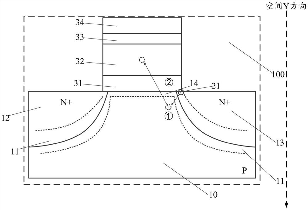
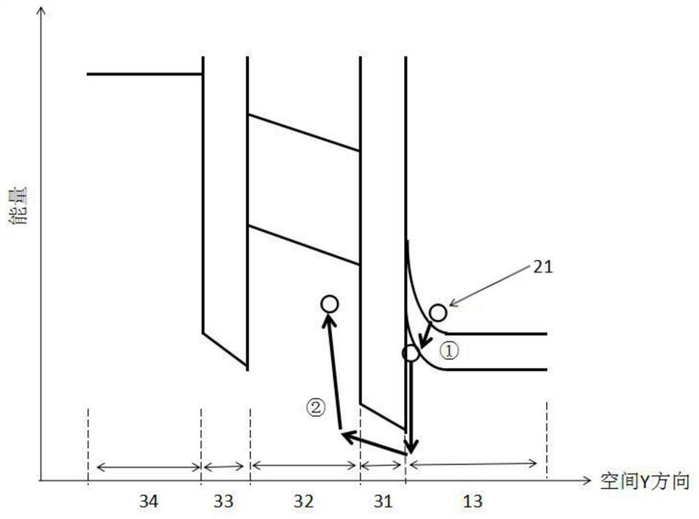
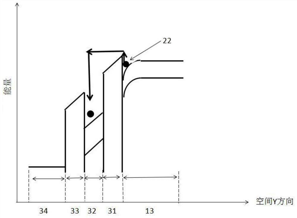
[0028] The present invention will be described in more detail below with reference to schematic diagrams and examples. The advantages and features of the present invention will be more apparent from the following description. It should be noted that all the drawings are in a very simplified form and use imprecise scales, and are only used to facilitate and clearly assist the purpose of illustrating the embodiments of the present invention.

[0029] In the following description, it will be understood that when a layer (or film), region, pattern or structure is referred to as being "on" a substrate, layer (or film), region and / or pattern, it can be directly on another layer or substrate, and / or intervening layers may also be present. Further, it will be understood that when a layer is referred to as being 'under' another layer, it can be directly under, and / or one or more intervening layers may also be present. In addition, designations regarding 'on' and 'under' each layer ma...


PUM


Abstract

The invention relates to a flash memory structure, comprising: a substrate, a source region, a drain region and a channel region between the source region and the drain region are arranged in the substrate, and the substrate and the channel adopt P-type Impurity doping, the source region and the drain region are doped with high-concentration N-type impurities; and a tunnel oxide layer, a charge storage layer, a blocking oxide layer and a control gate layer are sequentially stacked on the base of the channel region. The present invention utilizes back gate bias to assist band tunneling hot hole injection for programming, hot holes can enter the charge storage layer under the condition of low voltage difference to realize programming, and the requirement for capacitive coupling coefficient is relatively low. The channel electron injection method is used for erasing, and the electrons in the channel can also enter the charge storage layer under the condition of low voltage difference, so that the holes and electrons are combined one by one, and the holes entering the charge storage layer are gradually erased during programming. holes, avoiding the problems of erasing saturation and process window reduction caused by the high-voltage FN erasing mechanism in the prior art.

Description

technical field [0001] The invention relates to the field of semiconductors, in particular to a flash memory structure and corresponding programming, erasing and reading methods. Background technique [0002] In the prior art, the flash memory is usually programmed by using the BackBiasAssisted Band-to-Band Tunneling Induced Hot Electron Injection (B4-Flash) method , due to the introduction of the back gate bias to replace a part of the source-drain voltage, the voltage difference between the source and drain can be smaller than that of traditional flash memory, which is conducive to reducing the size of flash memory. The current B4-Flash flash memory structure is a p-type channel. [0003] The inventors found that, for the currently used p-type channel flash memory structure of B4-Flash, the electron tunneling effect of Fowler-Nordheim (FN) is usually used to erase the electrons in the charge storage layer. When erasing, it is necessary to apply a very large voltage diffe...

Claims


Application Information

Patent Timeline
Patent Type & Authority Patents(China)
IPC IPC(8): H01L29/792H01L29/788G11C16/10G11C16/14G11C16/26
CPCH01L29/7883H01L29/792G11C16/10G11C16/14G11C16/26
Inventor 顾经纶
Owner SHANGHAI HUALI MICROELECTRONICS CORP
Why Eureka
Try Eureka