


Quick Research
Generate reliable direction feasibility study reports for your R&D in just a few steps.

Technical Q&A
Discover and master advanced knowledge NOW. Basics, ideas, possibilities, all at once.

Find Solutions
As an expert in R&D theories, this can generate solutions to your technical problems instantly.

Evaluate Feasibility
Analyze your overall solution with one click, know your potential R&D risks in advance.

Monitor Landscape
Get weekly tech updates, stay abreast of the latest tech innovations and key insights.
Semiconductor structure and forming method thereof
A technology of semiconductor and fin structure, applied in the field of semiconductor structure and its formation
- Summary
- Abstract
- Description
- Claims
- Application Information
AI Technical Summary
Problems solved by technology
Method used
Image

Examples
Embodiment Construction
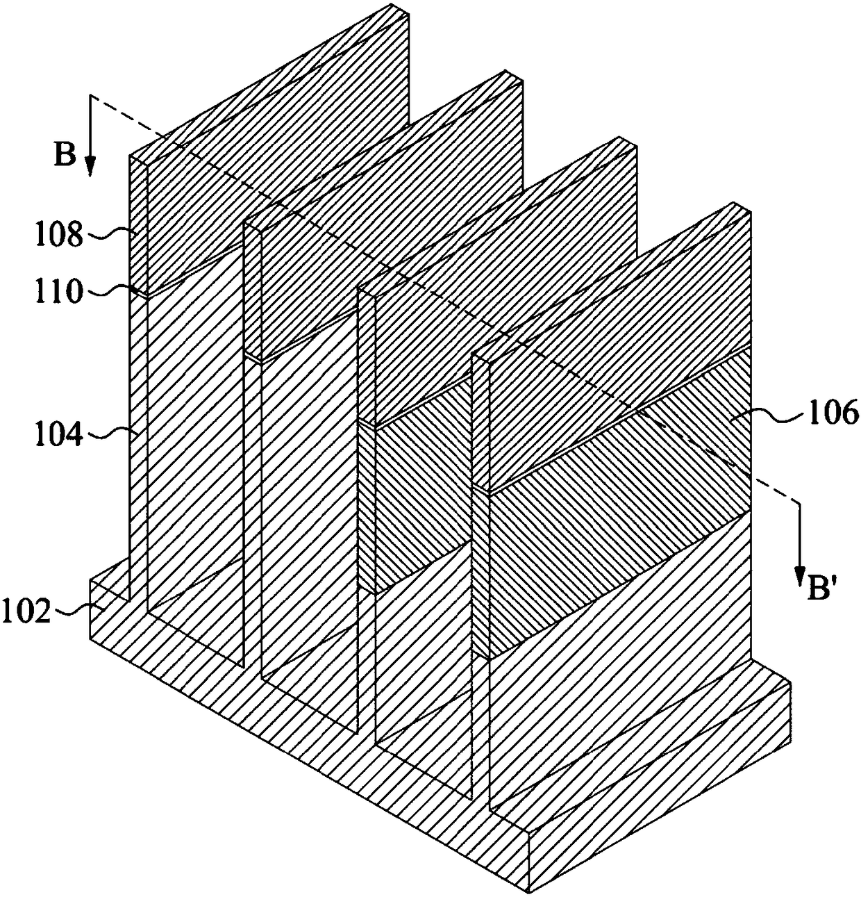
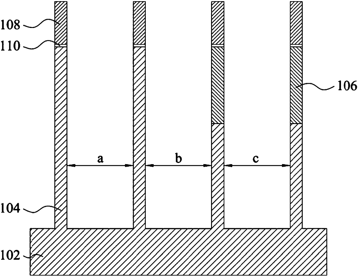
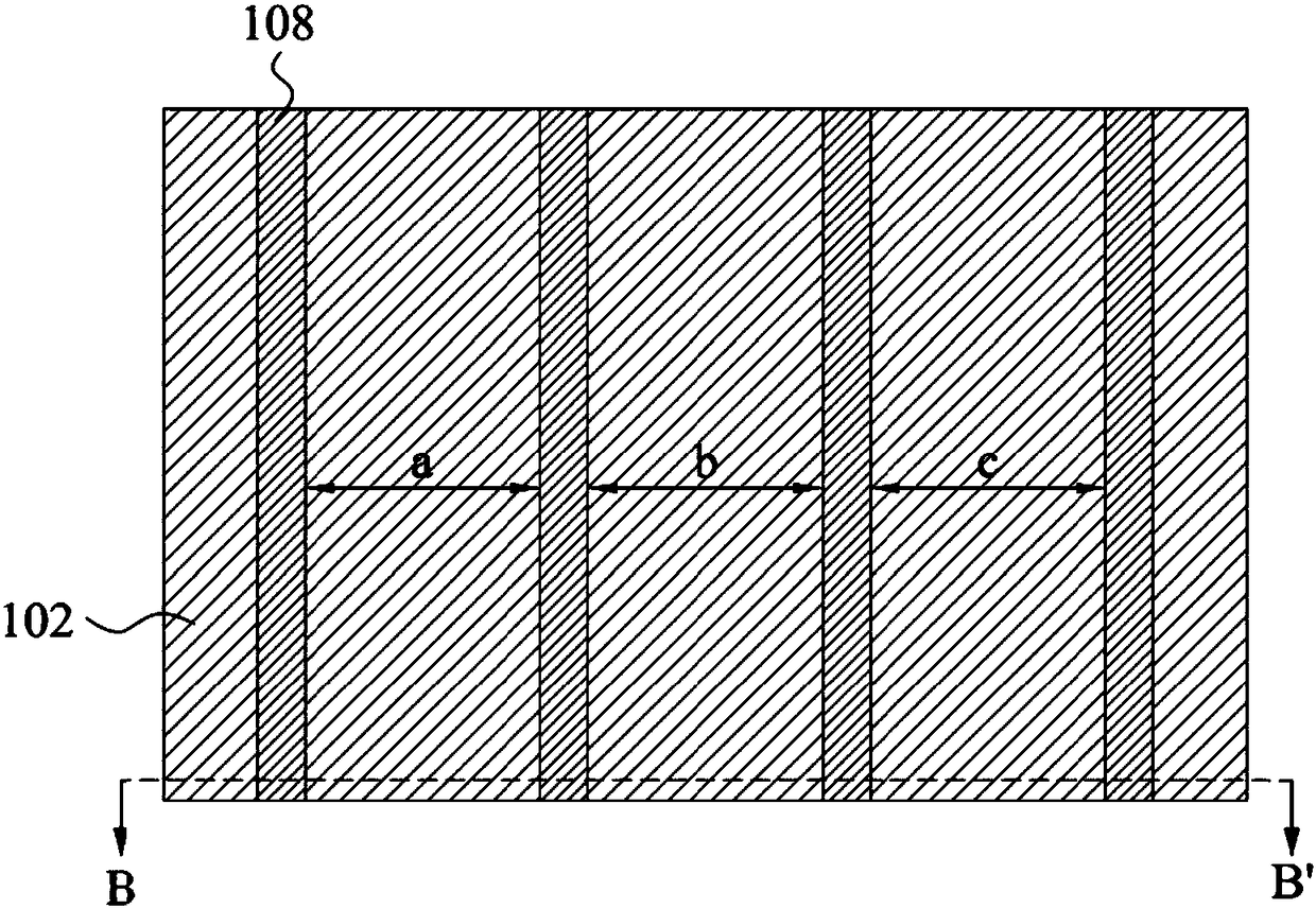
[0024] A number of implementations of the present disclosure will be disclosed in the following examples. For the sake of clarity, many practical details will be described together in the following description. However, it should be understood that these practical details should not be used to limit the present disclosure. That is to say, in some embodiments of the present disclosure, these practical details are unnecessary. In addition, for the sake of simplifying the drawings, some known and conventional structures and elements will be shown in a simple and schematic manner in the drawings. Also, the same reference numerals in different drawings may be considered as corresponding elements unless otherwise indicated. These figures are drawn to clearly express the connection relationship between the components in the embodiments, and do not show the actual size of the components.
[0025] In addition, relative spatial terms, such as "below", "lower", "bottom", "upper", and "...
PUM
| Property | Measurement | Unit |
|---|---|---|
| width | aaaaa | aaaaa |
| height | aaaaa | aaaaa |
| height | aaaaa | aaaaa |
Abstract
Description
Claims
Application Information
 - R&D Engineer
- R&D Manager
- IP Professional
- Industry Leading Data Capabilities
- Powerful AI technology
- Patent DNA Extraction
Browse by: Latest US Patents, China's latest patents, Technical Efficacy Thesaurus, Application Domain, Technology Topic, Popular Technical Reports.
© 2024 PatSnap. All rights reserved.Legal|Privacy policy|Modern Slavery Act Transparency Statement|Sitemap|About US| Contact US: help@patsnap.com