Thin film transistor device and manufacturing method thereof

A technology of thin film transistors and manufacturing methods, applied in the field of display substrates, capable of solving problems such as display failure

Active Publication Date: 2019-03-05
KUNSHAN GO VISIONOX OPTO ELECTRONICS CO LTD
View PDF6 Cites 2 Cited by
  • Summary
  • Abstract
  • Description
  • Claims
  • Application Information

AI Technical Summary

Problems solved by technology

[0005] In view of this, an embodiment of the present invention provides a thin film transistor device and a manufacturing method thereof, wh

Method used


Image

  • Thin film transistor device and manufacturing method thereof
  • Thin film transistor device and manufacturing method thereof
  • Thin film transistor device and manufacturing method thereof

Examples


Embodiment Construction

[0055] The following will clearly and completely describe the technical solutions in the embodiments of the present invention with reference to the accompanying drawings in the embodiments of the present invention. Obviously, the described embodiments are only some of the embodiments of the present invention, not all of them. Based on the embodiments of the present invention, all other embodiments obtained by persons of ordinary skill in the art without making creative efforts belong to the protection scope of the present invention.

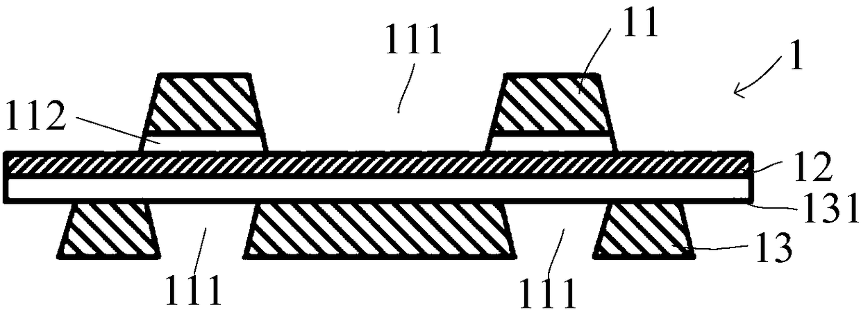
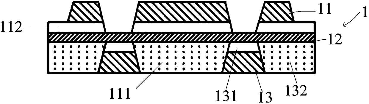
[0056] Figure 1a Shown is a schematic structural view of a thin film transistor device provided by an embodiment of the present invention, Figure 1b Shown is a projected schematic diagram of a gate electrode of a thin film transistor device provided by an embodiment of the present invention.

[0057] Such as Figure 1a As shown, the gate electrode 1 of the thin film transistor device may include a top gate 11 disposed above a channel layer 12 o...


PUM


Abstract

Embodiments of the invention provide a thin film transistor device and a manufacturing method thereof. A gate electrode of the thin film transistor device comprises a top gate and a bottom gate, wherein the top gate is arranged above a channel layer of the thin film transistor device; the bottom gate is arranged below the channel layer; at least one through hole is formed in the top gate, and theprojection, on a plane parallel to the channel layer, of the through hole in the top gate is covered by the projection, on the plane, of the top gate; and/or at least one through hole is formed in thebottom gate, and the projection, on the plane, of the through hole in the bottom gate is covered by the projection, on the plane, of the top gate. The thin film transistor device provided by the embodiments of the invention is capable of solving the problem of display failure caused by stress concentration when existing thin film transistor devices are bent to deform.

Description

technical field [0001] The invention relates to the technical field of display substrates, in particular to a thin film transistor device and a manufacturing method thereof. Background technique [0002] Flexible display devices are bendable and deformable display devices, and their display methods include thin-film transistor (TFT), organic electroluminescence (OLED), electrophoretic display (EPD), liquid crystal display (LCD) and other types. The deformable and bendable display substrate can bring subversive experience to users. [0003] During the bending or folding process of the flexible display device, the internal structure of the brittle thin film transistor device is easily broken, and the internal structure fracture of the thin film transistor device will affect the display effect or directly lead to malfunction. [0004] For the failure of thin film transistor devices due to bending or fracture, it is currently mentioned to open holes on the gate to release the s...

Claims


Application Information

Patent Timeline
IPC IPC(8): H01L29/786H01L29/423H01L21/336
CPCH01L29/42356H01L29/66742H01L29/786H01L29/78645
Inventor 王刚张露韩珍珍胡思明
Owner KUNSHAN GO VISIONOX OPTO ELECTRONICS CO LTD
Why Eureka
Try Eureka