Method for measuring S parameter and terminal equipment

A parameter and end face technology, which is applied in the field of microwave characteristic measurement of wafer-level semiconductor devices, can solve problems such as large random errors, and achieve the effect of improving measurement accuracy.

Active Publication Date: 2019-03-08
THE 13TH RES INST OF CHINA ELECTRONICS TECH GRP CORP
View PDF4 Cites 24 Cited by
  • Summary
  • Abstract
  • Description
  • Claims
  • Application Information

AI Technical Summary

Problems solved by technology

[0004] In view of this, the embodiment of the present invention provides a method and terminal equipment for detecting S parameters, which solves the influence of the crosstalk error term between probes and probes in the high-frequency

Method used


Image

  • Method for measuring S parameter and terminal equipment
  • Method for measuring S parameter and terminal equipment
  • Method for measuring S parameter and terminal equipment

Examples


Embodiment Construction

[0042] In the following description, specific details such as specific system structures and technologies are presented for the purpose of illustration rather than limitation, so as to thoroughly understand the embodiments of the present invention. It will be apparent, however, to one skilled in the art that the invention may be practiced in other embodiments without these specific details. In other instances, detailed descriptions of well-known systems, devices, circuits, and methods are omitted so as not to obscure the description of the present invention with unnecessary detail.

[0043] In order to illustrate the technical solutions of the present invention, specific examples are used below to illustrate.

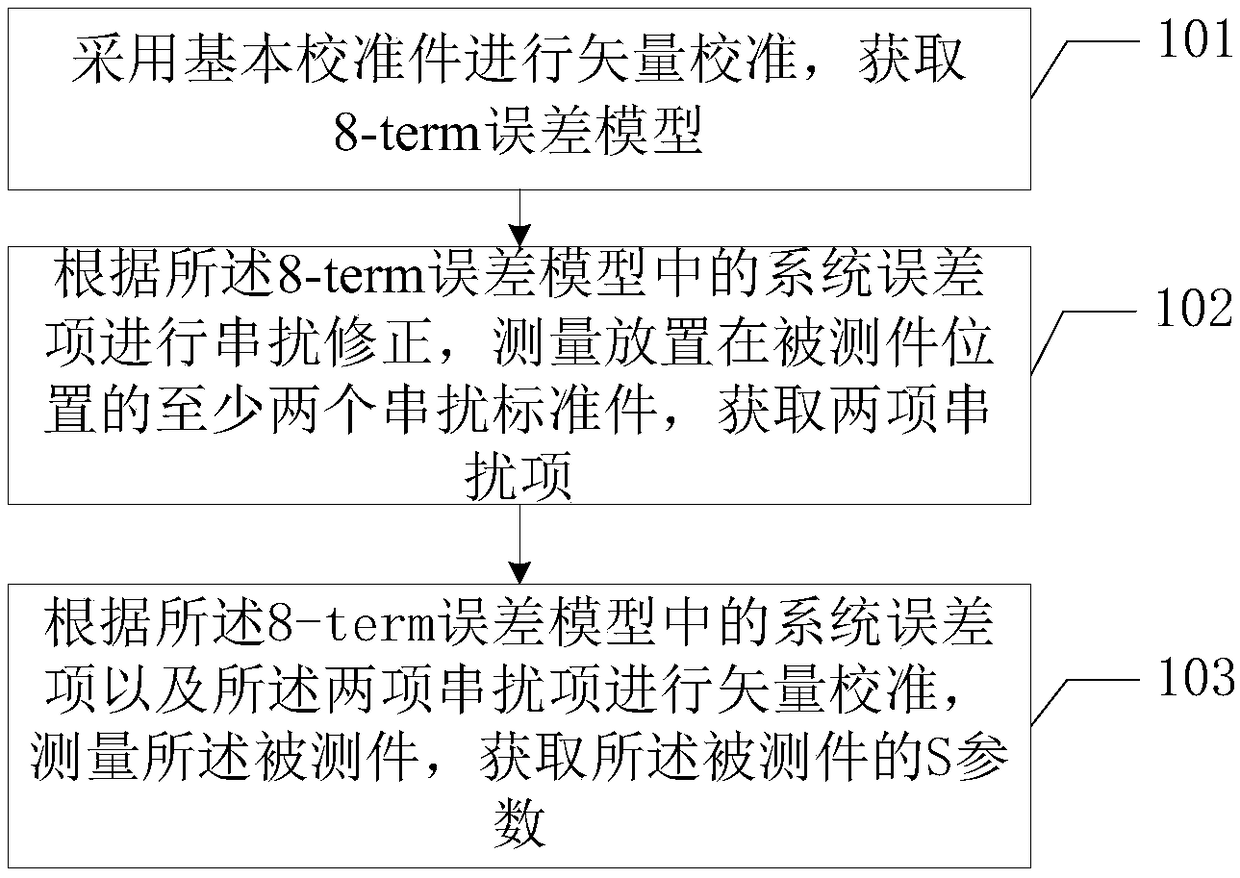
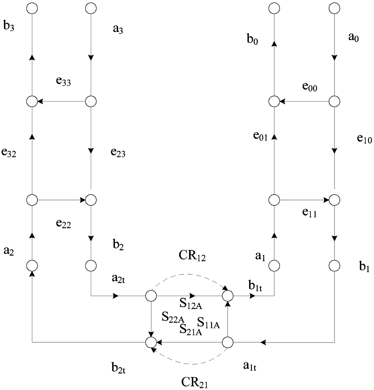
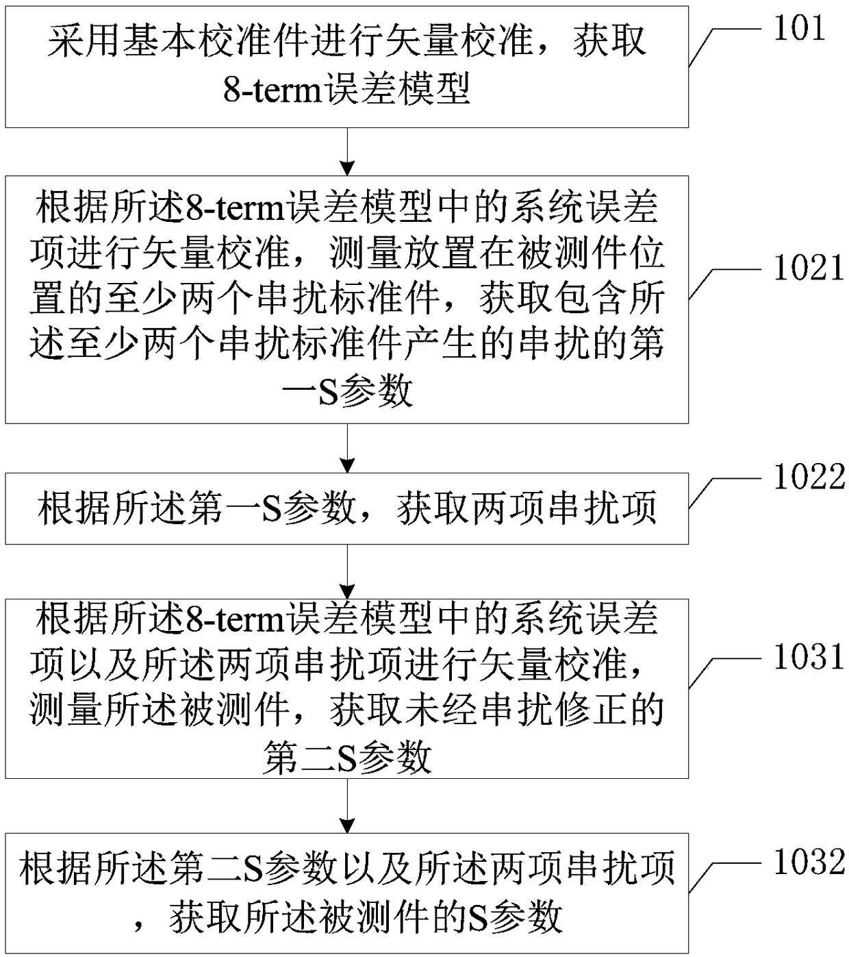
[0044] The embodiment of the present invention provides a method for detecting S parameters, the execution subject of the method may be an on-chip vector network analyzer, such as figure 1 As shown, the method includes the following steps:

[0045] In step 101, vector c...


PUM


Abstract

The invention is applicable to the technical field of measurement of microwave characteristics of wafer-level semiconductor devices, and provides a method for measuring an S parameter and terminal equipment. The method comprises the steps that vector calibration is conducted by using a basic calibration kit, and an 8-term error model is obtained; according to a system error item in the 8-term error model, crosstalk correction is conducted, at least two standard crosstalk pieces at the position of a to-be-measured piece are measured, and two crosstalk items are obtained; according to the systemerror item in the 8-term error model and the two crosstalk items, vector calibration is conducted, the to-be-measured piece is measured, and the S parameter of the to-be-measured piece is obtained. By means of the method, the problem about the influence of the crosstalk error items between probes in the high-frequency on-chip measurement process and the problem about a large random error caused by a single crosstalk standard in the crosstalk correction process can be solved, and the measurement accuracy of the high-frequency on-chip S parameter is further improved.

Description

technical field [0001] The invention belongs to the technical field of microwave characteristic measurement of wafer-level semiconductor devices, and in particular relates to a method for detecting S parameters and terminal equipment. Background technique [0002] A large number of "on-chip S-parameter test systems" equipped in the microelectronics industry require vector calibration of on-chip calibration components before use. The types of calibration components include SOLT (Short-Open-Load-Thru, short-circuit open-circuit load through), SOLR (Short-Open-Load-Reciprocal, short-circuit open-circuit load reciprocity), TRL (Thru-Reflect-Line, straight-through reflection line), LRM (Line-Reflect-Match, line reflection matching), LRRM (Line-Reflect-Reflect -Match, line reflection reflection matching), etc. Usually SOLT, SOLR, LRM, and LRRM use a 12-term error model, while TRL and MultilineTRL use an 8-term system error model. The calibration parts characterize the imperfecti...

Claims


Application Information

Patent Timeline
IPC IPC(8): G01R31/28
CPCG01R31/2822G01R31/287
Inventor 王一帮吴爱华梁法国刘晨栾鹏孙静霍烨
Owner THE 13TH RES INST OF CHINA ELECTRONICS TECH GRP CORP
Why Eureka
Try Eureka