Memory device

A memory, memory array technology, applied in information storage, static memory, digital memory information and other directions, can solve the problem of specification speed limit, too large gap, slow reading speed and so on

Active Publication Date: 2019-03-08
北京时代全芯存储技术股份有限公司
View PDF11 Cites 0 Cited by
  • Summary
  • Abstract
  • Description
  • Claims
  • Application Information

AI Technical Summary

Problems solved by technology

There are at least two main problems in the existing memory architecture: (1) The reference circuit is located in the read-write circuit, generally a transistor is used to generate a reference current, and the position of the transistor is different from the position of the memory unit (cell) If the value is too large, the currents generated by the positions of different memory cells are slightly different, which causes the value set by the reference current to have different noise margins for judging the data of the memory cell as "1" or "0" noisemargin), can not produce memory optimal effect
The variation mechanism of the resistance of the memory cell is different from that of the transistor, so the reference current cannot accurately and adaptively match the variation of the memory cell
(2) In the prior art, because the read-write circuit is located around the column decoding circuit, when reading the memory unit (cell), due to the loading effect of the bit line, the memory unit farthest from the read-out circuit The reading speed is the slowest, and the specification speed of the entire memory is limited by the slowest memory unit

Method used


Image

  • Memory device
  • Memory device
  • Memory device

Examples


Embodiment Construction

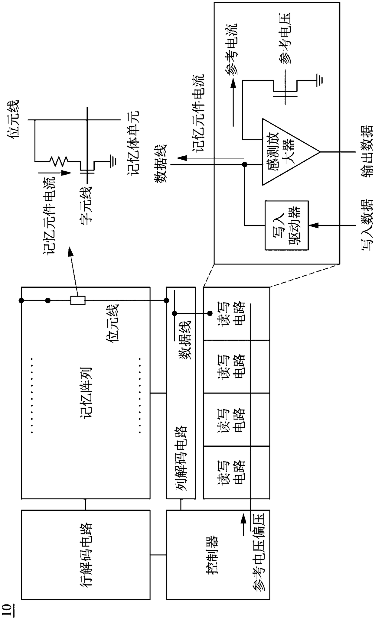
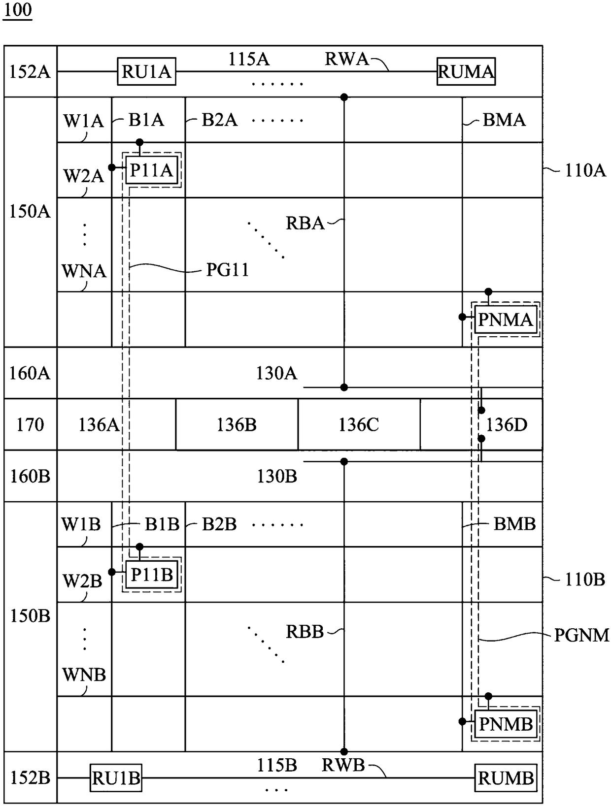
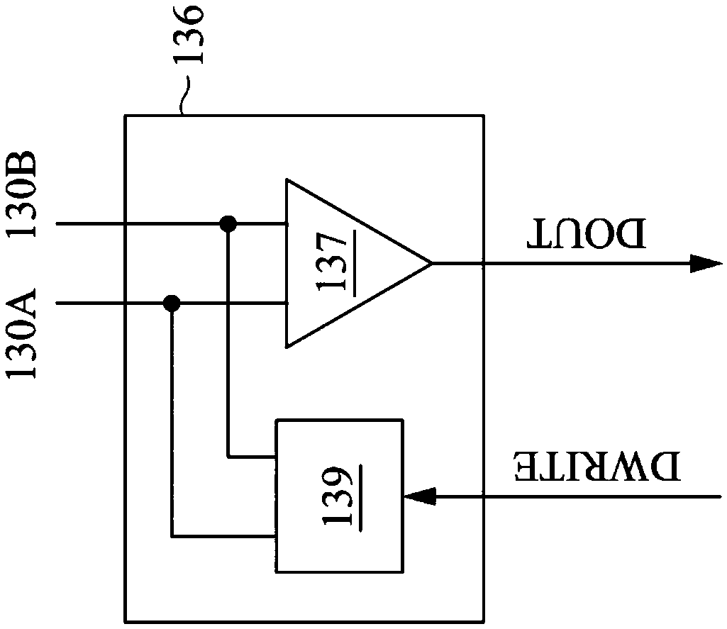
[0021] The following is a detailed description of the embodiments in conjunction with the attached drawings to better understand the aspect of the case, but the provided embodiments are not intended to limit the scope of the disclosure, and the description of the structure and operation is not intended to The order of execution is limited, and any device with equivalent functions produced by recombining components is within the scope of the present disclosure. In addition, according to industry standards and common practice, the drawings are only for the purpose of assisting explanation, and are not drawn according to original scale. In fact, the dimensions of various features can be arbitrarily increased or decreased for the convenience of illustration. In the following description, the same components will be described with the same symbols for easy understanding.

[0022] Unless otherwise specified, the terms used throughout the specification and claims generally have the o...


PUM


Abstract

A memory device comprises a first memory array, a second memory array, a first bit line driving circuit, a second bit line driving circuit, a first word line driving circuit, a second word line driving circuit, a read-write circuit, a controller, a first reference driving circuit and a second reference driving circuit. The first memory array and the second memory array comprise a plurality of memory units. The first bit line driving circuit and the second bit line driving circuit are used for interpreting a memory bit address and driving a bit line. The first and second word line driving circuits are used for interpreting a memory word address and driving a word line. The read-write circuit is used for reading, writing or resetting the memory unit. The controller is used for switching thefirst memory array and the second memory array to work in a single-memory unit mode or a double-memory unit mode. The first reference driving circuit and the second reference driving circuit are usedfor driving reference lines. The embodiment of the invention can be adjusted to a single-memory unit mode or a double-memory unit mode according to requirements.

Description

technical field [0001] The present disclosure relates to a memory device, in particular to a phase change memory memory device. Background technique [0002] In memory technology, memristive memory includes phase change memory (Phase change memory, PCM), which can change the resistance value of the element through the crystal phase change of its own material, and store information with the change of resistance value. When the material is in a crystalline state, it exhibits a low resistance value, on the contrary, when it is in an amorphous state, it exhibits a high resistance value, thereby storing data such as "1" or "0". [0003] In the prior art, when reading the data of the memory unit in the memory device, the single memory unit is turned on, and the current corresponding to the single memory unit is compared with the reference current to obtain It is determined whether the data stored in the single memory unit is "1" or "0". However, the comparison by the current val...

Claims


Application Information

Patent Timeline
Patent Type & Authority Applications(China)
IPC IPC(8): G11C13/00
CPCG11C13/0009G11C13/0021G11C13/0069G11C13/003G11C2213/79G11C13/004G11C13/0023G11C13/0026G11C13/0028G11C2013/0054G11C7/14G11C7/1069G11C7/1096G11C7/1045Y02D10/00G11C11/00G11C11/419G11C13/0004
Inventor 吴瑞仁简汎宇黄圣财郑君华
Owner 北京时代全芯存储技术股份有限公司
Why Eureka
Try Eureka