A sensor monocrystalline silicon etching device with uniform etching

An etching device and monocrystalline silicon technology, applied in the field of sensors, can solve the problems of poor etching effect and low etching efficiency, and achieve the effect of sufficient etching and improved efficiency

Active Publication Date: 2021-06-29
蚌埠市龙子湖区金力传感器厂
View PDF6 Cites 0 Cited by
  • Summary
  • Abstract
  • Description
  • Claims
  • Application Information

AI Technical Summary

Problems solved by technology

[0003] In view of the above-mentioned shortcomings of the prior art, the object of the present invention is to provide a sensor single crystal silicon etching device with uniform etching, which is used to solve the problem that only one side of the sensor single crystal silicon can be etched. Efficient etching, poor etching effect and low etching efficiency on the other side

Method used


Image

  • A sensor monocrystalline silicon etching device with uniform etching
  • A sensor monocrystalline silicon etching device with uniform etching
  • A sensor monocrystalline silicon etching device with uniform etching

Examples


Embodiment 1

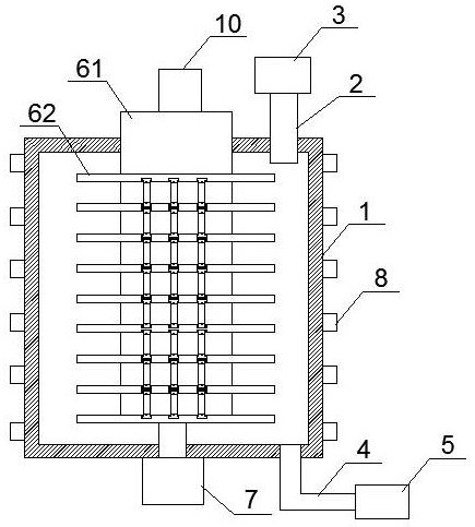
[0020] like Figure 1-3 As shown, the present invention discloses a sensor monocrystalline silicon etching device with uniform etching, which includes a reaction chamber 1, and an upper end of the reaction chamber 1 is provided with a gas supply pipe 2, which is connected to the gas supply pipe 2 arranged outside the reaction chamber 1. The source chamber 3, the lower end of the reaction chamber 3 is provided with a suction pipe 4, which is connected to a vacuum pump 5 arranged outside the reaction chamber; the axial position of the reaction chamber 1 is provided with a sheet holder 6, which is connected to the reaction chamber. 1 the output shaft of the external servo motor 7; the outer side of the reaction chamber 1 is provided with an electromagnetic coil 8;

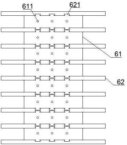
[0021] The film holder 6 consists of a hollow cylindrical rotating column 61 and a circular ring plate 62 that is uniformly and fixedly connected to the outer wall of the rotating column, and the lower end of the rota...

Embodiment 2

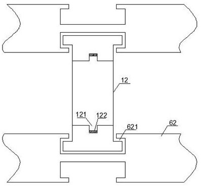
[0029] As a further improvement: According to [ image 3 ], the inner wall of the card slot 121 is provided with an elastic rubber pad 122 . The improved advantage of this embodiment is to prevent the single crystal silicon wafer from being damaged by the card board 12 .

[0030] The remaining features and advantages of this embodiment are the same as those of the first embodiment.

Embodiment 3

[0032] As a further improvement: the width of one end of the horizontal rod on the card board 12 away from the U-shaped plate on the card board 12 is greater than the diameter of the sliding hole 611 . The improved advantage of this embodiment is that the clamping rod 12 is prevented from being separated from the sliding hole 611 .

[0033] The remaining features and advantages of this embodiment are the same as those of the second embodiment.


PUM


Abstract

The present invention relates to the technical field of sensors, in particular to a sensor monocrystalline silicon etching device with uniform etching. The lower end is sealed; the outer wall of the rotating column between two adjacent circular plates is evenly provided with a number of sliding holes of equal height, and the sliding holes are connected with the inner wall of the rotating column; the opposite surfaces of each adjacent two circular plates are uniformly There are a number of chute slots corresponding to the positions; the sliding hole is slidably connected with a clamping plate passing through the sliding hole, and the clamping plate is used to fix the monocrystalline silicon wafer; the clamping plate slides with the corresponding chute on the two adjacent ring plates Connection, the invention has the advantages of convenient use, improved etching efficiency, improved etching effect, and reduced labor intensity of workers.

Description

technical field [0001] The invention relates to the technical field of sensors, in particular to a sensor monocrystalline silicon etching device with uniform etching. Background technique [0002] In the process of processing single-crystal silicon for sensors, it needs to be etched; in the existing etching process, it is often done by stacking multiple single-crystal silicon on the wafer frame, and passing them to the wafer frame. The reactive gas is introduced at the location, and the reactive gas generates plasma in the electric field environment to etch the single crystal silicon; the wafer holder usually needs to be rotated during the etching process to increase the contact uniformity between the single crystal silicon and the plasma However, in the current etching process, single-crystal silicon wafers are stacked on the wafer frame. During the etching process of the stacked single-crystal silicon wafers, the single-crystal silicon can only be Effective etching is per...

Claims


Application Information

Patent Timeline
Patent Type & Authority Patents(China)
IPC IPC(8): H01L21/67H01L21/3065H01J37/32
CPCH01J37/32431H01J37/32715H01L21/3065H01L21/67069
Inventor 张如根
Owner 蚌埠市龙子湖区金力传感器厂
Why Eureka
Try Eureka