
Wafer processing method

A processing method and wafer technology, which is applied in the field of WL-CSP wafer processing, can solve the problems of poor device precision and the pattern of the device wafer is not exposed on the periphery, and achieve the effect of a simple alignment process

Pending Publication Date: 2019-03-26
DISCO CORP
View PDF5 Cites 0 Cited by
  • Summary
  • Abstract
  • Description
  • Claims
  • Application Information

AI Technical Summary

Problems solved by technology

[0012] However, the device accuracy is generally poor on the periphery of the wafer. When alignment is performed based on the pattern exposed on the periphery of the wafer, the wafer may be divided at a position separated from the planned division line, and there are still devices due to differences in wafers. When the pattern of the wafer is not exposed on the outer periphery

Method used


Image

  • Wafer processing method
  • Wafer processing method
  • Wafer processing method

Examples


Embodiment Construction

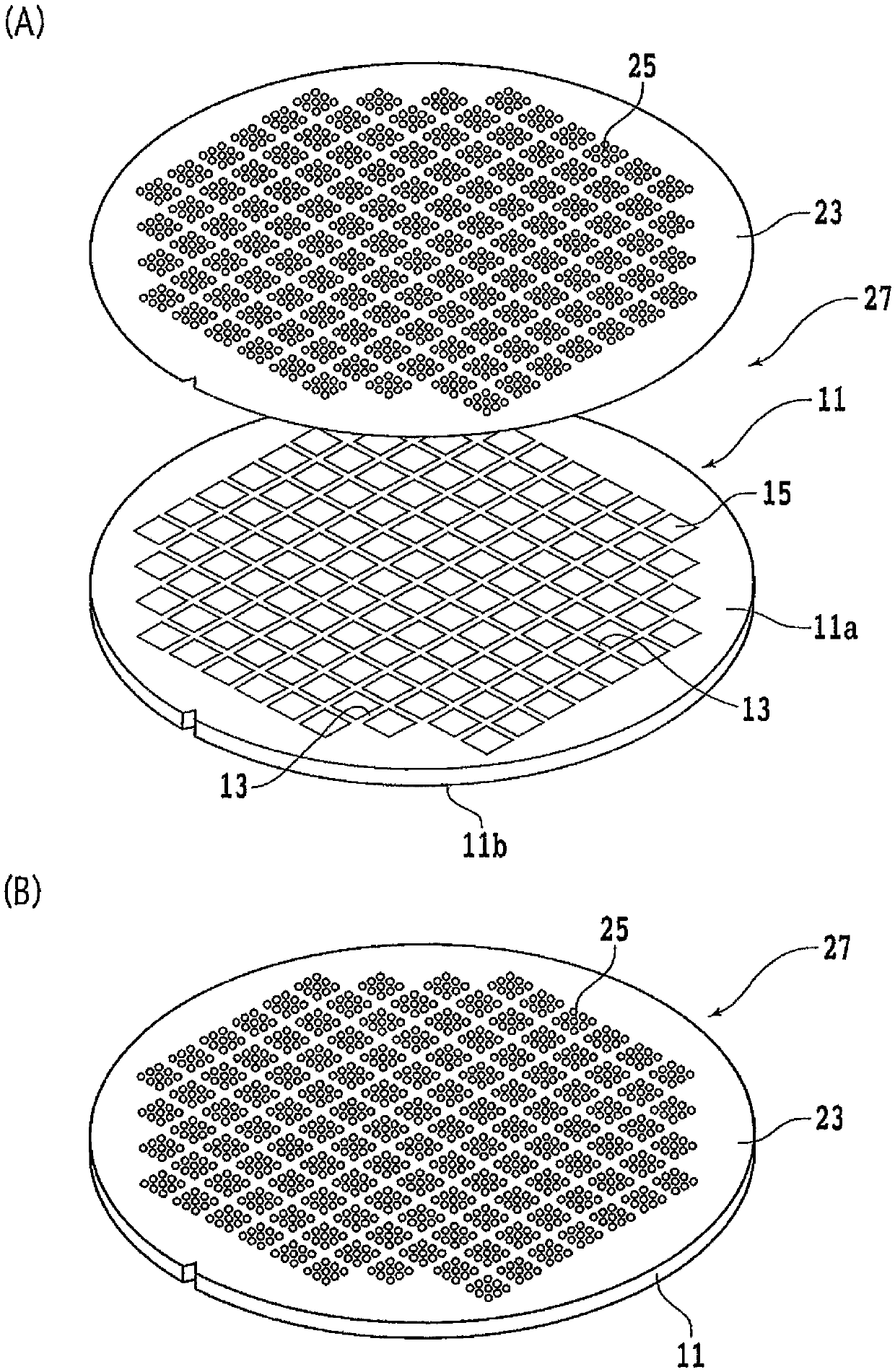
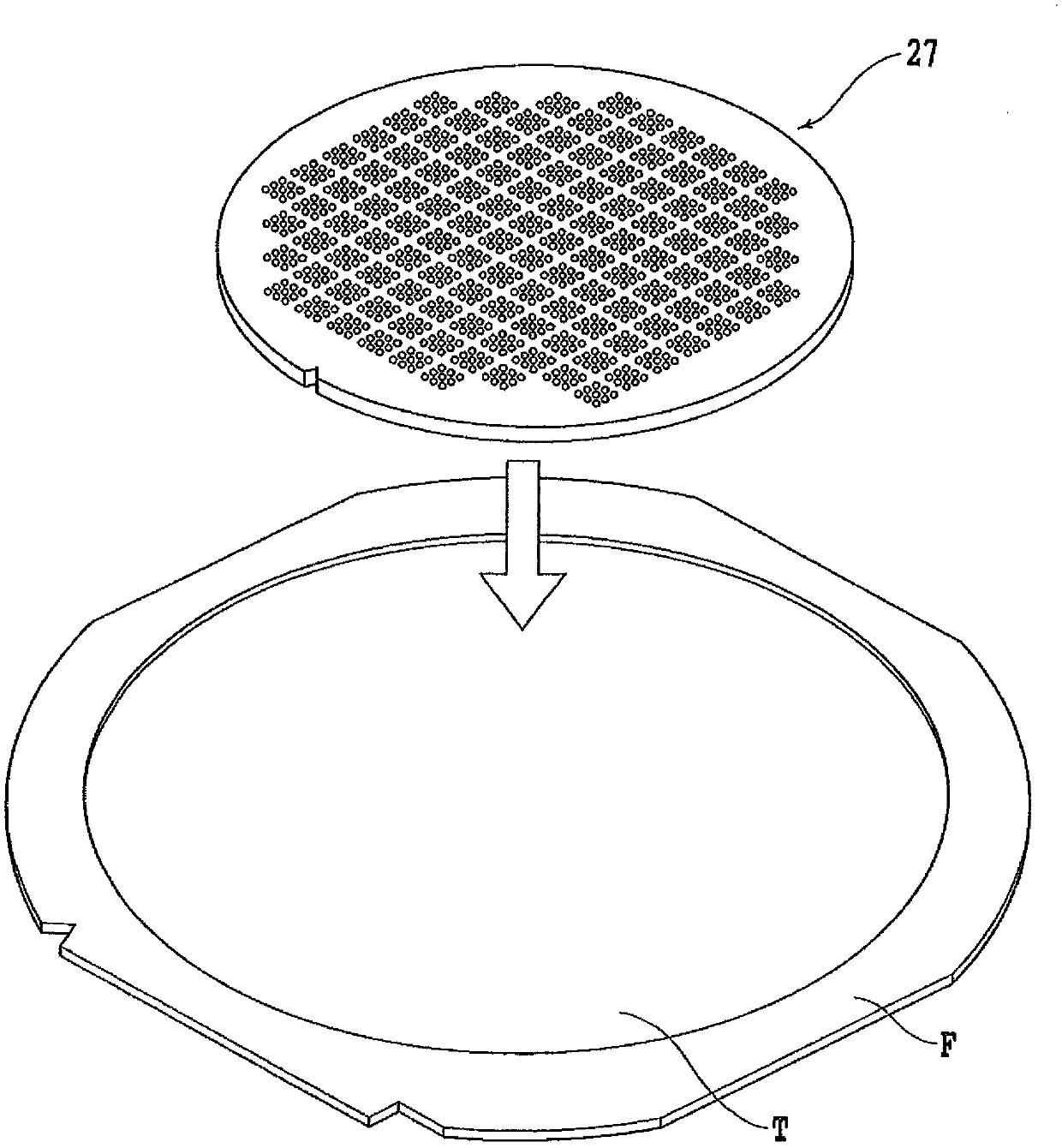
[0023] Hereinafter, embodiments of the present invention will be described in detail with reference to the drawings. refer to figure 1 (A) shows an exploded perspective view of the WL-CSP wafer 27 . figure 1 (B) is a perspective view of the WL-CSP wafer 27 .

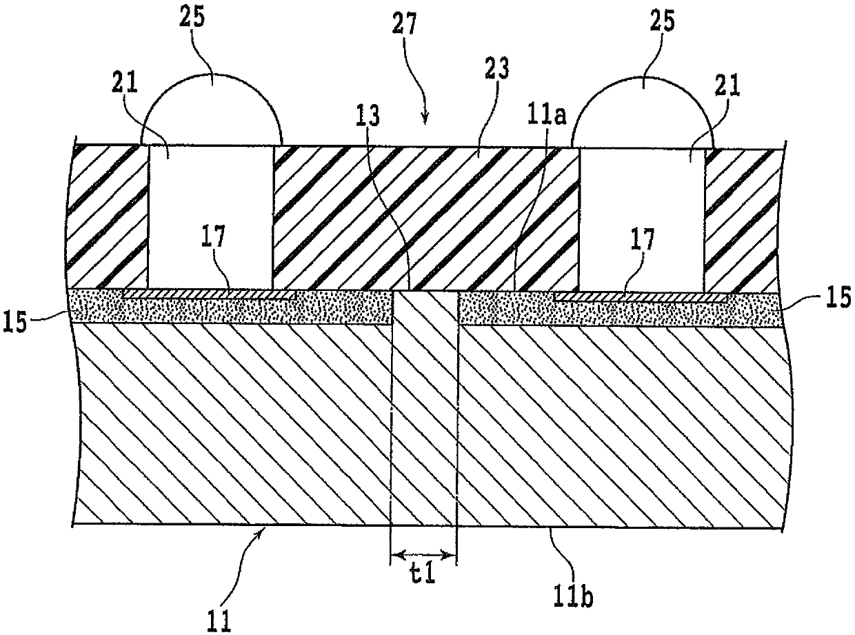
[0024] Such as figure 1 As shown in (A), on the front surface 11 a of the device wafer 11 , devices 15 such as LSIs are formed in regions divided by a plurality of dividing lines (streets) 13 formed in a lattice.

[0025] The back surface 11b of the device wafer (hereinafter, sometimes simply referred to as wafer) 11 is ground in advance to thin it to a predetermined thickness (about 100 μm to 200 μm), and then, as figure 2 As shown, after forming a plurality of metal pillars 21 electrically connected to the electrodes 17 in the device 15 , the front side 11 a side of the wafer 11 is sealed with a sealing material 23 in such a way that the metal pillars 21 are embedded.

[0026] The composition of the sealing materi...


PUM

PropertyMeasurementUnit
thicknessaaaaaaaaaa

Abstract

A wafer processing method is provided for aligning the wafer through a carbon black encapsulated sealing material on the front of the wafer. According to the wafer processing method, a front surface of the wafer is sealed with a sealing member and a plurality of bumps are formed individually in the chip regions of the sealing member includes an alignment step of picking up an image of a front surface side of the wafer through the sealing member by an infrared image pickup unit from the front surface side of the wafer to detect alignment marks and detecting a scheduled division line to be cut based on the alignment marks, and a division step of cutting the wafer along the scheduled division line from the front surface side of the wafer by a cutting blade to divide the wafer into individualdevice chips sealed at the front surface thereof with the sealing member. The sealing member has such transparency that infrared rays to be received by the infrared image pickup unit pass the sealingmember.

Description

technical field [0001] The invention relates to a processing method of a WL-CSP wafer. Background technique [0002] WL-CSP (Wafer-level Chip Size Package: Wafer-level Chip Size Package) wafer refers to forming a redistribution layer or electrodes (metal pillars) in the wafer state, sealing the front side with resin, and dividing it into The technology of each package is widely used from the viewpoint of miniaturization and weight reduction because the size of a package obtained by singulating a wafer is the size of a chip of a semiconductor device. [0003] In the manufacturing process of the WL-CSP wafer, a rewiring layer is formed on the device surface side of the device wafer with multiple devices formed, and then the metal pillars connected to the electrodes in the device are formed through the rewiring layer, and then the metal pillars are sealed with resin. and device sealing. [0004] Next, after thinning the sealing material and exposing the metal post on the fron...

Claims


Application Information

Patent Timeline
Patent Type & Authority Applications(China)
IPC IPC(8): H01L21/78H01L21/67H01L21/66B23K26/53
CPCB23K26/53H01L21/67259H01L21/78H01L22/20H01L21/67092H01L21/681B28D5/0029B28D5/0064H01L21/6836H01L2221/68327H01L2224/11
Inventor 铃木克彦伴祐人
Owner DISCO CORP
Features
  • Generate Ideas
  • Intellectual Property
  • Life Sciences
  • Materials
  • Tech Scout
  • Unparalleled Data Quality
  • Higher Quality Content
  • 60% Fewer Hallucinations
Learn More