
Method of processing wafer

A processing method and wafer technology, applied in metal processing, stone processing equipment, metal processing equipment, etc., can solve problems such as poor productivity and time-consuming, and achieve the effect of a simple alignment process

Pending Publication Date: 2019-03-15
DISCO CORP
View PDF7 Cites 0 Cited by
  • Summary
  • Abstract
  • Description
  • Claims
  • Application Information

AI Technical Summary

Problems solved by technology

[0013] However, in the alignment method described in the above publication, instead of the cutting tool for dicing, it is necessary to attach a wide cutting tool for edge trimming to the spindle to remove the sealing material on the outer peripheral portion of the wafer. It takes time and labor to replace the cutting tool and remove the sealing material on the outer peripheral part by edge trimming, and there is a problem of poor productivity

Method used


Image

  • Method of processing wafer
  • Method of processing wafer
  • Method of processing wafer

Examples


Embodiment Construction

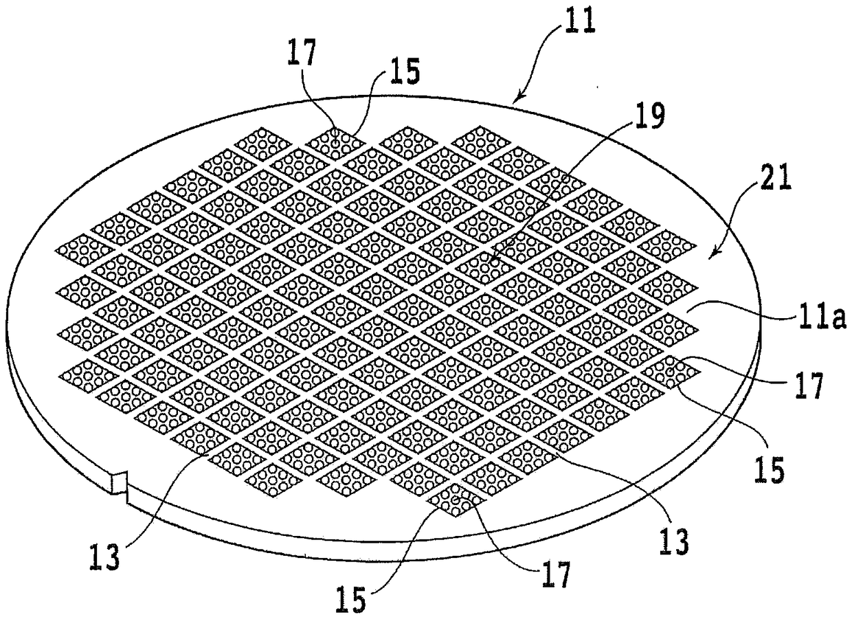
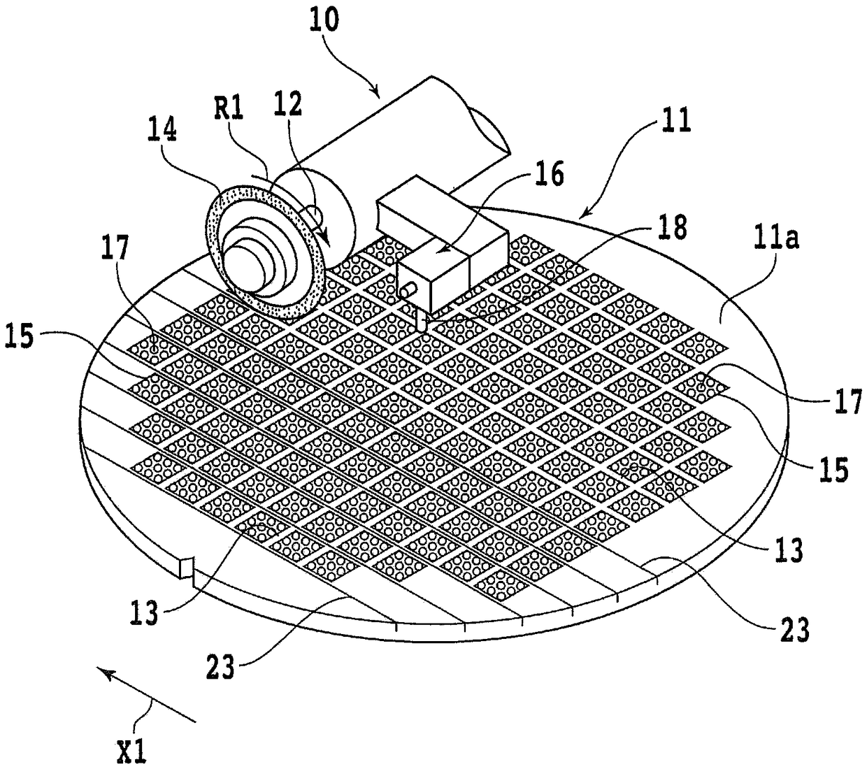
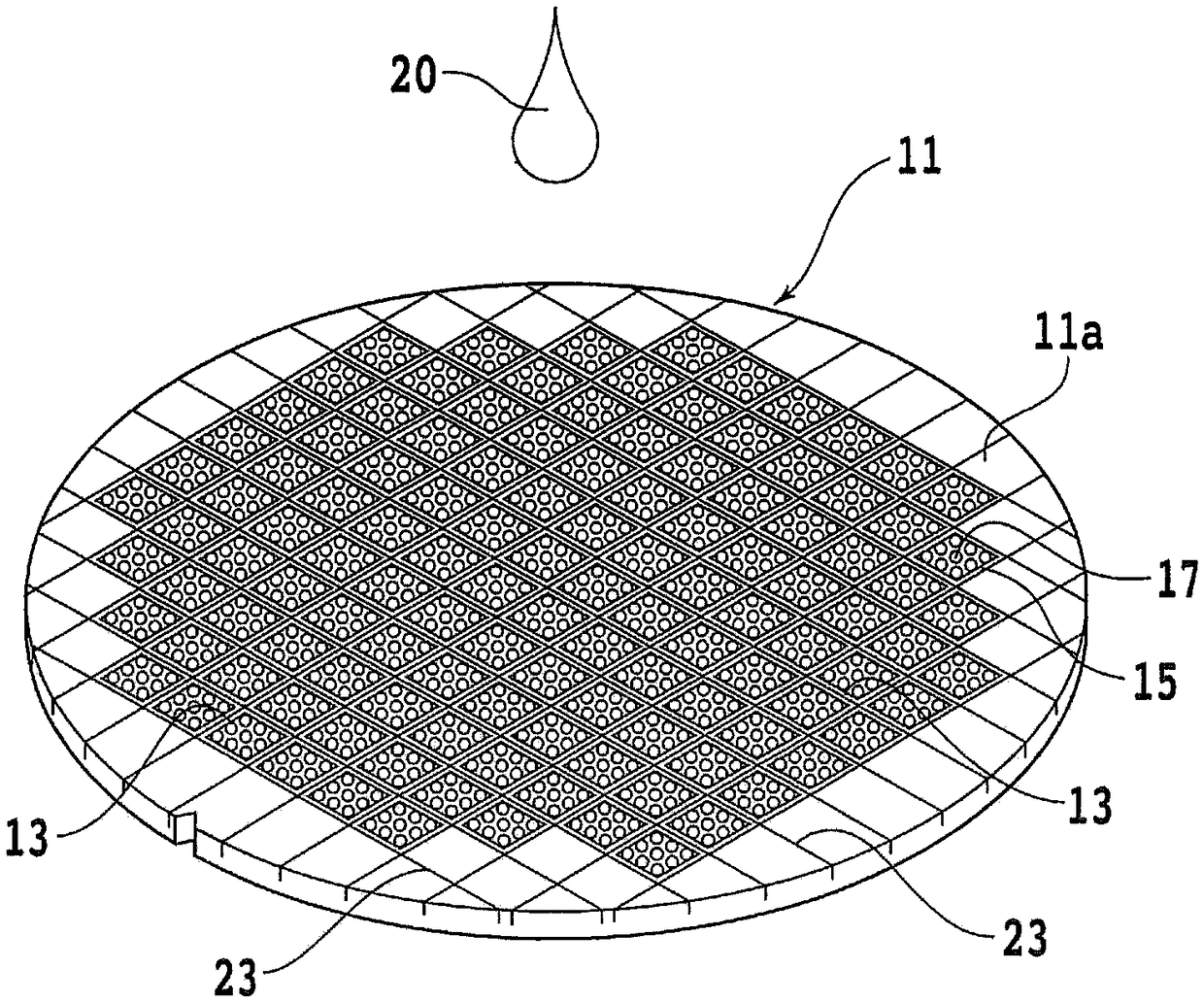
[0030] Hereinafter, embodiments of the present invention will be described in detail with reference to the drawings. refer to figure 1 , shows a front perspective view of a semiconductor wafer (hereinafter, sometimes simply referred to as a wafer) 11 suitable for processing by the processing method of the present invention.

[0031] On the front surface 11 a of the semiconductor wafer 11 , a plurality of dividing lines (streets) 13 are formed in a grid pattern. Devices 15 such as ICs and LSIs are formed in each region partitioned by vertical dividing lines 13 .

[0032] There are a plurality of electrode bumps (hereinafter, sometimes simply referred to as bumps) 17 on the front surface of each device 15, and the wafer 11 has on its front surface: a device region 19, which is formed with a plurality of devices each having a plurality of bumps 17 15 ; and a peripheral remaining region 21 surrounding the device region 19 .

[0033] In the wafer processing method according to t...


PUM


Abstract

A method of processing a wafer is provided. The method includes a cutting groove forming step of forming a cutting groove having a depth corresponding to a thickness of a device chip from a front sideof the wafer along a predetermined dividing line; a sealing step of sealing the front surface of the wafer with a sealing material; a grinding step of grinding the wafer from the back side of the wafer to the finished thickness to expose the sealing material in the cutting groove; an alignment step of detecting an alignment mark by an infrared ray imaging member photographing the front side of the wafer from the front side of the wafer through the sealing material, and detecting a predetermined dividing line for laser processing according to the alignment mark; a modified layer forming step of positioning the condensing point of the laser beam having a wavelength of transparency to the sealing material inside the sealing material in the cutting groove to radiate the laser beam to form a modified layer; and a dividing step of applying an external force to the sealing material in the cutting groove and dividing the wafer into respective device chips with a front surface and four side surfaces surrounded by the sealing material with the modified layer as a dividing starting point.

Description

technical field [0001] The invention relates to a wafer processing method, and the wafer is processed to form a 5S mold package. Background technique [0002] As a structure to achieve miniaturization and high-density mounting of various devices such as LSI and NAND flash memory, for example, a chip size package (CSP) in which device chips are packaged in chip sizes has been put into practical use, And it is widely used in mobile phones, smart phones, etc. In addition, among these CSPs, in recent years, a CSP that seals not only the front surface of a chip but also the entire side surface of a chip with a sealing material, that is, a so-called 5S molded package, has been developed and put into practical use. [0003] Conventional 5S molded packages are produced through the following steps. [0004] (1) External connection terminals called devices (circuits) and bumps are formed on the front surface of a semiconductor wafer (hereinafter, sometimes roughly referred to as a w...

Claims


Application Information

Patent Timeline
Patent Type & Authority Applications(China)
IPC IPC(8): H01L21/304
CPCH01L21/3043B23K26/0823H01L23/544B23K26/364B23K2101/40B23K2103/42B24B7/228B28D5/022H01L21/78H01L2223/54453H01L2223/54426H01L21/6836H01L2221/68327H01L2221/6834H01L21/561H01L23/3114H01L21/67092H01L23/29H01L21/67132H01L2924/181H01L2224/11H01L2924/00012H01L21/76H01L21/565H01L21/68H01L27/146
Inventor 铃木克彦伴祐人
Owner DISCO CORP
Features
  • Generate Ideas
  • Intellectual Property
  • Life Sciences
  • Materials
  • Tech Scout
  • Unparalleled Data Quality
  • Higher Quality Content
  • 60% Fewer Hallucinations
Learn More